JAJSF03K September   2011  – December 2023 LMK03806

PRODUCTION DATA  

  1.   1
  2. 特長
  3. アプリケーション
  4. 概要
  5. Pin Configuration and Functions
  6. Specifications
    1. 5.1 Absolute Maximum Ratings
    2. 5.2 ESD Ratings
    3. 5.3 Recommended Operating Conditions
    4. 5.4 Thermal Information
    5. 5.5 Electrical Characteristics
    6. 5.6 Timing Requirements
    7. 5.7 Typical Characteristics
  7. Parameter Measurement Information
    1. 6.1 Differential Voltage Measurement Terminology
  8. Detailed Description
    1. 7.1 Overview
    2. 7.2 Functional Block Diagrams
    3. 7.3 Features Description
      1. 7.3.1 Serial MICROWIRE Timing Diagram and Terminology
      2. 7.3.2 Crystal Support With Buffered Outputs
      3. 7.3.3 Integrated Loop Filter Poles
      4. 7.3.4 Integrated VCO
      5. 7.3.5 Clock Distribution
        1. 7.3.5.1 CLKout DIvider
        2. 7.3.5.2 Programmable Output Type
        3. 7.3.5.3 Clock Output Synchronization
      6. 7.3.6 Default Start-Up Clocks
    4. 7.4 Device Functional Modes
    5. 7.5 Programming
      1. 7.5.1 General Information
        1. 7.5.1.1 Special Programming Case for R0 to R5 for CLKoutX_Y_DIV > 25
        2. 7.5.1.2 Recommended Initial Programming Sequence
        3. 7.5.1.3 READBACK
          1. 7.5.1.3.1 Readback Example
  9. Application and Implementation
    1. 8.1 Application Information
      1. 8.1.1 Crystal Interface
      2. 8.1.2 Driving OSCin Pins With a Single-Ended Source
      3. 8.1.3 Driving OSCin Pins With a Differential Source
      4. 8.1.4 Frequency Planning With the LMK03806
      5. 8.1.5 Configuring the PLL
        1. 8.1.5.1 Example PLL Configuration
      6. 8.1.6 Digital Lock Detect
    2. 8.2 Typical Application
      1. 8.2.1 Design Requirements
      2. 8.2.2 Detailed Design Procedure
        1. 8.2.2.1 Device Selection
          1. 8.2.2.1.1 Clock Architect
          2. 8.2.2.1.2 Clock Design Tool
          3. 8.2.2.1.3 Calculation Using LCM
        2. 8.2.2.2 Device Configuration
        3. 8.2.2.3 PLL Loop Filter Design
          1. 8.2.2.3.1 Example Loop Filter Design
        4. 8.2.2.4 Other Device Specific Configuration
          1. 8.2.2.4.1 Digital Lock Detect
        5. 8.2.2.5 Device Programming
      3. 8.2.3 Application Curves
    3. 8.3 System Examples
      1. 8.3.1 System Level Diagram
    4. 8.4 Best Design Practices
      1. 8.4.1 LVCMOS Complementary vs. Non-Complementary Operation
      2. 8.4.2 LVPECL Outputs
      3. 8.4.3 Sharing MICROWIRE (SPI) Lines
      4. 8.4.4 SYNC Pin
      5. 8.4.5 CLKout Vcc Pins
    5. 8.5 Power Supply Recommendations
      1. 8.5.1 Current Consumption and Power Dissipation Calculations
    6. 8.6 Layout
      1. 8.6.1 Layout Guidelines
      2. 8.6.2 Layout Example
  10. Device and Documentation Support
    1. 9.1 Device Support
      1. 9.1.1 Development Support
    2. 9.2 Documentation Support
      1. 9.2.1 Related Documentation
    3. 9.3 ドキュメントの更新通知を受け取る方法
    4. 9.4 サポート・リソース
    5. 9.5 Trademarks
    6. 9.6 静電気放電に関する注意事項
    7. 9.7 用語集
  11. 10Register Maps
    1. 10.1  Default Device Register Settings After Power On Reset
    2. 10.2  Register R0 TO R5
      1. 10.2.1 CLKoutX_Y_PD, Powerdown CLKoutX_Y Output Path
      2. 10.2.2 RESET
      3. 10.2.3 POWERDOWN
      4. 10.2.4 CLKoutX_Y_DIV, Clock Output Divide
    3. 10.3  Registers R6 TO R8
      1. 10.3.1 CLKoutX_TYPE
    4. 10.4  REGISTER R9
    5. 10.5  REGISTER R10
      1. 10.5.1 OSCout1_TYPE, LVPECL Output Amplitude Control
      2. 10.5.2 OSCout0_TYPE
      3. 10.5.3 EN_OSCoutX, OSCout Output Enable
      4. 10.5.4 OSCoutX_MUX, Clock Output Mux
      5. 10.5.5 OSCout_DIV, Oscillator Output Divide
    6. 10.6  REGISTER R11
      1. 10.6.1 NO_SYNC_CLKoutX_Y
      2. 10.6.2 SYNC_POL_INV
      3. 10.6.3 SYNC_TYPE
      4. 10.6.4 EN_PLL_XTAL
    7. 10.7  REGISTER R12
      1. 10.7.1 LD_MUX
      2. 10.7.2 LD_TYPE
      3. 10.7.3 SYNC_PLL_DLD
    8. 10.8  REGISTER R13
      1. 10.8.1 READBACK_TYPE
      2. 10.8.2 GPout0
    9. 10.9  REGISTER 14
      1. 10.9.1 GPout1
    10. 10.10 REGISTER 16
    11. 10.11 REGISTER 24
      1. 10.11.1 PLL_C4_LF, PLL Integrated Loop Filter Component
      2. 10.11.2 PLL_C3_LF, PLL Integrated Loop Filter Component
      3. 10.11.3 PLL_R4_LF, PLL Integrated Loop Filter Component
      4. 10.11.4 PLL_R3_LF, PLL Integrated Loop Filter Component
    12. 10.12 REGISTER 26
      1. 10.12.1 EN_PLL_REF_2X, PLL Reference Frequency Doubler
      2. 10.12.2 PLL_CP_GAIN, PLL Charge Pump Current
      3. 10.12.3 PLL_DLD_CNT
    13. 10.13 REGISTER 28
      1. 10.13.1 PLL_R, PLL R Divider
    14. 10.14 REGISTER 29
      1. 10.14.1 OSCin_FREQ, PLL Oscillator Input Frequency Register
      2. 10.14.2 PLL_N_CAL, PLL N Calibration Divider
    15. 10.15 REGISTER 30
      1. 10.15.1 PLL_P, PLL N Prescaler Divider
      2. 10.15.2 PLL_N, PLL N Divider
    16. 10.16 REGISTER 31
      1. 10.16.1 READBACK_ADDR
      2. 10.16.2 uWire_LOCK
  12. 11Revision History
  13. 12Mechanical, Packaging, and Orderable Information

パッケージ・オプション

メカニカル・データ(パッケージ|ピン)
サーマルパッド・メカニカル・データ
発注情報

Digital Lock Detect

The digital lock detect circuit is used to determine the lock status of the PLL. The flowchart in Figure 8-6 shows the general way this circuit works.

EVENTPLLWINDOW SIZE (ε)LOCK COUNT
PLL LockedPLL3.7 nsPLL_DLD_CNT

For a digital lock detect event to occur there must be a number of PLL phase detector cycles during which the time/phase error of the PLL_R reference and PLL_N feedback signal edges are within the 3.7 ns window size of the LMK03806. Lock count is the term which is used to specify how many PLL phase detector cycles have been within the window size of 3.7 ns at any given time. Since there must be a specified number phase detector events before a lock event occurs, a minimum digital lock event time can be calculated as lock count / Fpd.
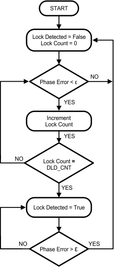
GUID-5CAF334E-05E2-4AC2-80F5-6DDAD9011A30-low.gifFigure 8-6 Digital Lock Detect Flow Diagram

A user specified ppm accuracy for lock detect is programmable using a lock count register. By using Equation 8, values for a lock count and window size can be chosen to set the frequency accuracy required by the system in ppm before the digital lock detect event occurs. Units of Fpd are Hertz:

Equation 8. GUID-570F5AAD-4B0D-4BC3-A6A4-6E198DCF5985-low.gif

The effect of the lock count value is that it shortens the effective lock window size by dividing the window size by lock count.

If at any time the PLL_R reference and PLL_N feedback signals are outside the time window set by window size, then the lock count value is reset to 0.

For example, we will calculate the minimum PLL digital lock time given a PLL Fpd of 40 MHz and PLL_DLD_CNT = 10,000. The minimum lock time of PLL will be 10,000 / 40 MHz = 250 µs.