SNAS489K March 2011 – December 2014 LMK04803 , LMK04805 , LMK04806 , LMK04808
PRODUCTION DATA.
- 1 Features
- 2 Applications
- 3 Description
- 4 Revision History
- 5 Pin Configuration and Functions
- 6 Specifications
-
7 Parameter Measurement Information
- 7.1
Charge Pump Current Specification Definitions
- 7.1.1 Charge Pump Output Current Magnitude Variation Vs. Charge Pump Output Voltage
- 7.1.2 Charge Pump Sink Current Vs. Charge Pump Output Source Current Mismatch
- 7.1.3 Charge Pump Output Current Magnitude Variation vs. Ambient Temperature"Temperature" to "Ambient Temperature" in heading titled "Charge Pump Output Current Magnitude Variation vs. Ambient Temperature"
- 7.2 Differential Voltage Measurement Terminology
- 7.1
Charge Pump Current Specification Definitions
-
8 Detailed Description
- 8.1
Overview
- 8.1.1 System Architecture
- 8.1.2 PLL1 Redundant Reference Inputs (CLKin0/CLKin0* and CLKin1/CLKin1*)
- 8.1.3 PLL1 Tunable Crystal Support
- 8.1.4 VCXO/CRYSTAL Buffered Outputs
- 8.1.5 Frequency Holdover
- 8.1.6 Integrated Loop Filter Poles
- 8.1.7 Internal VCO
- 8.1.8 External VCO Mode
- 8.1.9 Clock Distribution
- 8.1.10 0-Delay
- 8.1.11 Default Startup Clocks
- 8.1.12 Status Pins
- 8.1.13 Register Readback
- 8.2 Functional Block Diagram
- 8.3
Feature Description
- 8.3.1 Serial MICROWIRE Timing Diagram
- 8.3.2 Advanced MICROWIRE Timing Diagrams
- 8.3.3 Inputs / Outputs
- 8.3.4 Input Clock Switching
- 8.3.5 Holdover Mode
- 8.3.6 PLLs
- 8.3.7 Status Pins
- 8.3.8 VCO
- 8.3.9
Clock Distribution
- 8.3.9.1 Fixed Digital Delay
- 8.3.9.2 Fixed Digital Delay - Example
- 8.3.9.3
Clock Output Synchronization (SYNC)
- 8.3.9.3.1 Effect of SYNC
- 8.3.9.3.2 Methods of Generating SYNC
- 8.3.9.3.3 Avoiding Clock Output Interruption Due to Sync
- 8.3.9.3.4 SYNC Timing
- 8.3.9.3.5
Dynamically Programming Digital Delay
- 8.3.9.3.5.1 Absolute vs. Relative Dynamic Digital Delay
- 8.3.9.3.5.2 Dynamic Digital Delay and 0-Delay Mode
- 8.3.9.3.5.3 SYNC and Minimum Step Size
- 8.3.9.3.5.4 Programming Overview
- 8.3.9.3.5.5 Internal Dynamic Digital Delay Timing
- 8.3.9.3.5.6 Other Timing Requirements
- 8.3.9.3.5.7 Absolute Dynamic Digital Delay
- 8.3.9.3.5.8 Relative Dynamic Digital Delay
- 8.3.10 0-Delay Mode
- 8.4 Device Functional Modes
- 8.5 Programming
- 8.6
Register Maps
- 8.6.1 Register Map and Readback Register Map
- 8.6.2 Default Device Register Settings After Power On Reset
- 8.6.3
Register Descriptions
- 8.6.3.1
Register R0 TO R5
- 8.6.3.1.1 CLKoutX_Y_PD, Powerdown CLKoutX_Y Output Path
- 8.6.3.1.2 CLKoutX_Y_OSCin_Sel, Clock Group Source
- 8.6.3.1.3 CLKoutY_ADLY_SEL[29], CLKoutX_ADLY_SEL[28], Select Analog Delay
- 8.6.3.1.4 CLKoutX_Y_DDLY, Clock Channel Digital Delay
- 8.6.3.1.5 Reset
- 8.6.3.1.6 POWERDOWN
- 8.6.3.1.7 CLKoutX_Y_HS, Digital Delay Half Shift
- 8.6.3.1.8 CLKoutX_Y_DIV, Clock Output Divide
- 8.6.3.2 Registers R6 TO R8
- 8.6.3.3
Register R10
- 8.6.3.3.1 OSCout1_LVPECL_AMP, LVPECL Output Amplitude Control
- 8.6.3.3.2 OSCout0_TYPE
- 8.6.3.3.3 EN_OSCoutX, OSCout Output Enable
- 8.6.3.3.4 OSCoutX_MUX, Clock Output Mux
- 8.6.3.3.5 PD_OSCin, OSCin Powerdown Control
- 8.6.3.3.6 OSCout_DIV, Oscillator Output Divide
- 8.6.3.3.7 VCO_MUX
- 8.6.3.3.8 EN_FEEDBACK_MUX
- 8.6.3.3.9 VCO_DIV, VCO Divider
- 8.6.3.3.10 FEEDBACK_MUX
- 8.6.3.4 Register R11
- 8.6.3.5 Register R12
- 8.6.3.6 Register R13
- 8.6.3.7 Register 14
- 8.6.3.8 REGISTER 15
- 8.6.3.9 Register 16
- 8.6.3.10 Register 23
- 8.6.3.11
Register 24
- 8.6.3.11.1 PLL2_C4_LF, PLL2 Integrated Loop Filter Component
- 8.6.3.11.2 PLL2_C3_LF, PLL2 Integrated Loop Filter Component
- 8.6.3.11.3 PLL2_R4_LF, PLL2 Integrated Loop Filter Component
- 8.6.3.11.4 PLL2_R3_LF, PLL2 Integrated Loop Filter Component
- 8.6.3.11.5 PLL1_N_DLY
- 8.6.3.11.6 PLL1_R_DLY
- 8.6.3.11.7 PLL1_WND_SIZE
- 8.6.3.12 Register 25
- 8.6.3.13 Register 26
- 8.6.3.14 REGISTER 27
- 8.6.3.15 Register 28
- 8.6.3.16 Register 29
- 8.6.3.17 Register 30
- 8.6.3.18 Register 31
- 8.6.3.1
Register R0 TO R5
- 8.1
Overview
-
9 Application and Implementation
- 9.1
Application Information
- 9.1.1 Loop Filter
- 9.1.2 Driving CLKin and OSCin Inputs
- 9.1.3 Termination and Use of Clock Output (Drivers)
- 9.1.4 Frequency Planning with the LMK0480x Family
- 9.1.5 PLL Programming
- 9.1.6 Digital Lock Detect Frequency Accuracy
- 9.1.7 Calculating Dynamic Digital Delay Values for any Divide
- 9.1.8 Optional Crystal Oscillator Implementation (OSCin/OSCin*)
- 9.1.9 Application Curves
- 9.2 Typical Applications
- 9.3 System Examples
- 9.4 Do's and Don'ts
- 9.1
Application Information
- 10Power Supply Recommendations
- 11Layout
- 12Device and Documentation Support
- 13Mechanical, Packaging, and Orderable Information
パッケージ・オプション
メカニカル・データ(パッケージ|ピン)
- NKD|64
サーマルパッド・メカニカル・データ
- NKD|64
発注情報
1 Features
- Ultra-Low RMS Jitter Performance
- 111 fs RMS Jitter (12 kHz to 20 MHz)
- 123 fs RMS Jitter (100 Hz to 20 MHz)
- Dual Loop PLLatinum™ PLL Architecture
- PLL1
- Integrated Low-Noise Crystal Oscillator Circuit
- Holdover Mode when Input Clocks are Lost
- Automatic or Manual Triggering/Recovery
- PLL2
- Normalized PLL Noise Floor of –227 dBc/Hz
- Phase Detector Rate up to 155 MHz
- OSCin Frequency-Doubler
- Integrated Low-Noise VCO
- 2 Redundant Input Clocks with LOS
- Automatic and Manual Switch-Over Modes
- 50 % Duty Cycle Output Divides, 1 to 1045 (Even and Odd)
- 12 LVPECL, LVDS, or LVCMOS Programmable Outputs
- Digital Delay: Fixed or Dynamically Adjustable
- 25 ps Step Analog Delay Control.
- 14 Differential Outputs. Up to 26 Single Ended.
- Up to 6 VCXO/Crystal Buffered Outputs
- Clock Rates of up to 1536 MHz
- 0-Delay Mode
- Three Default Clock Outputs at Power Up
- Multi-Mode: Dual PLL, Single PLL, and Clock Distribution
- Industrial Temperature Range: –40 to 85°C
- 3.15-V to 3.45-V Operation
- 2 Dedicated Buffered/Divided OSCin Clocks
- Package: 64-Pin WQFN (9.0 × 9.0 × 0.8 mm)
2 Applications
- Data Converter Clocking
- Wireless Infrastructure
- Networking, SONET/SDH, DSLAM
- Medical / Video / Military / Aerospace
- Test and Measurement
3 Description
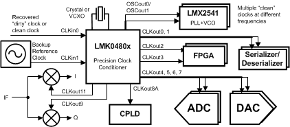
The LMK0480x family is the industry's highest performance clock conditioner with superior clock jitter cleaning, generation, and distribution with advanced features to meet next generation system requirements. The dual loop PLLatinum™ architecture is capable of 111 fs rms jitter (12 kHz to 20 MHz) using a low noise VCXO module or sub-200 fs rms jitter (12 kHz to 20 MHz) using a low cost external crystal and varactor diode.
The dual loop architecture consists of two high-performance phase-locked loops (PLL), a low-noise crystal oscillator circuit, and a high-performance voltage controlled oscillator (VCO). The first PLL (PLL1) provides low-noise jitter cleaner functionality while the second PLL (PLL2) performs the clock generation. PLL1 can be configured to either work with an external VCXO module or the integrated crystal oscillator with an external tunable crystal and varactor diode. When paired with a very narrow loop bandwidth, PLL1 uses the superior close-in phase noise (offsets below 50 kHz) of the VCXO module or the tunable crystal to clean the input clock. The output of PLL1 is used as the clean input reference to PLL2 where it locks the integrated VCO. The loop bandwidth of PLL2 can be optimized to clean the far-out phase noise (offsets above 50 kHz) where the integrated VCO outperforms the VCXO module or tunable crystal used in PLL1.
Device Information
| PART NUMBER | VCO FREQUENCY | REFERENCE INPUTS |
|---|---|---|
| LMK04803 | 1840 to 2030 MHz | 2 |
| LMK04805 | 2148 to 2370 MHz | |
| LMK04806 | 2370 to 2600 MHz | |
| LMK04808 | 2750 to 3072 MHz |
- For all available packages, see the orderable addendum at the end of the datasheet.
Simplified Schematic
4 Revision History
Changes from J Revision (March 2013) to K Revision
- Changed 90 to 80 and 80 to 90 for fCLKout-startup parameter in Electrical CharacteristicsGo
- Added "Specification is not valid for CLKoutX or CLKoutY in analog delay mode" in table note for Electrical CharacteristicsGo
- Changed "Temperature" to "Ambient Temperature" in heading titled "Charge Pump Output Current Magnitude Variation vs. Ambient Temperature" Go
- Added "temporarily" in VCXO/CRYSTAL Buffered OutputsGo
- Changed from "n possible" to "D possible" in 0-DelayGo
- Changed "can" to "cannot" in Input Clock Switching - Pin Select ModeGo
- Deleted Clock Switch Event without Holdover in Clock Switch Event with HoldoverGo
- Added paragraph beginning "For applications ..." in PLL2 Frequency DoublerGo
- Changed 5 to15 in Table 11Go
- Deleted Mode 5 row in Table 12Go
- Added Mode 15 Additional Configurations section Go
- In Table 16, added [27:26], [23:22], and [21:20] for Register 27 row. Added [31:20] for R28. Added [26:24] for R30. Added [7:6].Go
- In Table 18, changed "Actual PLL2 N divider value used in calibration routine". Added footnote "Inversion for Status 0 and 1 pins is only valid for CLKin_SELECT_MODE = 0x06"Go
- In Table 28, added "to reduce supply..." footnote for 9 through 14. Added footnote "To reduce supply switching and crosstalk noise, it is recommended to use a complementary LVCMOS output type such as 6 or 7".Go
- Added footnote "To reduce supply" for 8 through 14 in Table 32Go
- Changed "Divide" to "Definition" in Table 39, Table 40, Table 61, and Table 62Go
- Changed to "MUX OUTPUT" in Table header row in Table 42Go
- In Table 43, added footnote, "Contact TI Applications for more information on using this mode". Changed to "Dual PLL, External VCO (Fin), 0-Delay" for 15 (0x0F)Go
- Added "Inversion for Status 0 and 1 pins is only valid for CLKin_SELECT_MODE = 0x06" in CLKin_Sel_INVGo
- In FORCE_HOLDOVER, added "(EN_TRACK = 0 or 1, EN_MAN_DAC =1)". Added "(EN_TRACK = 1, EN_MAN_DAC = 0, EN_VTUNE_RAIL_DET = 0)"Go
- Changed to R[23:14] in DAC_CNTGo
- In Table 90, added (0x0000), (0x0001), (0x0002), (0x0003). Changed "Divide" to "Value" in the header row.Go
- Added (0x00) through (0x04) in Table 91Go
- Added PLL2 Frequency DoublerGo
- Changed from "Divide" to "Value" in Table 95Go
- Added PLL2 Frequency Doubler reference in Table 103Go
- Added note "Unless in 0-delay..." in PLL2_N_CAL, PLL2 N Calibration DividerGo
- Changed "Mode_MUX1" to "VCO_MUX" in PLL2_P, PLL2 N Prescaler DividerGo
- Changed "register" to "Defintion" in table header row for Table 110Go
- Updated Minimum Digital Lock Detect Time Calculation ExampleGo
- Added "Performance of other LMK0480x devices will be similar" in Optional Crystal Oscillator Implementation (OSCin/OSCin*)Go
- Changed to "(fs rms)" in Table 125Go
- Added text in red for Figure 40Go
- In Vcc2, Vcc3, Vcc10, Vcc11, Vcc12, Vcc13 (CLKout Vccs), added bullet point starting with "It is recommended..." Changed ≤ 10 MHz to ≤ 30 MHzGo
- Added paragraph "It is recommended..." in Vcc5 (CLKin and OSCout1), Vcc7 (OSCin and OSCout0)Go
- Added Mode = 15. Removed Mode = 5 in Table 127Go
- Deleted "of about 2 square inches" in Layout GuidelinesGo
Changes from I Revision (March 2013) to J Revision
- Changed layout of National Data Sheet to TI formatGo