JAJSTE0 March 2024 LMK05318B-Q1
PRODUCTION DATA
- 1
- 1 特長
- 2 アプリケーション
- 3 概要
- 4 Pin Configuration and Functions
- 5 Specifications
- 6 Parameter Measurement Information
-
7 Detailed Description
- 7.1 Overview
- 7.2 Functional Block Diagram
- 7.3
Feature Description
- 7.3.1 Oscillator Input (XO_P/N)
- 7.3.2 Reference Inputs (PRIREF_P/N and SECREF_P/N)
- 7.3.3 Clock Input Interfacing and Termination
- 7.3.4 Reference Input Mux Selection
- 7.3.5 Hitless Switching
- 7.3.6 Gapped Clock Support on Reference Inputs
- 7.3.7 Input Clock and PLL Monitoring, Status, and Interrupts
- 7.3.8
PLL Relationships
- 7.3.8.1 PLL Frequency Relationships
- 7.3.8.2 Analog PLLs (APLL1, APLL2)
- 7.3.8.3 APLL Reference Paths
- 7.3.8.4 APLL Phase Frequency Detector (PFD) and Charge Pump
- 7.3.8.5 APLL Feedback Divider Paths
- 7.3.8.6 APLL Loop Filters (LF1, LF2)
- 7.3.8.7 APLL Voltage Controlled Oscillators (VCO1, VCO2)
- 7.3.8.8 APLL VCO Clock Distribution Paths (P1, P2)
- 7.3.8.9 DPLL Reference (R) Divider Paths
- 7.3.8.10 DPLL Time-to-Digital Converter (TDC)
- 7.3.8.11 DPLL Loop Filter (DLF)
- 7.3.8.12 DPLL Feedback (FB) Divider Path
- 7.3.9 Output Clock Distribution
- 7.3.10 Output Channel Muxes
- 7.3.11 Output Dividers (OD)
- 7.3.12 Clock Outputs (OUTx_P/N)
- 7.3.13 Glitchless Output Clock Start-Up
- 7.3.14 Clock Output Interfacing and Termination
- 7.3.15 Output Synchronization (SYNC)
- 7.4 Device Functional Modes
- 7.5 Programming
- 8 Application and Implementation
- 9 Device and Documentation Support
- 10Revision History
- 11Mechanical, Packaging, and Orderable Information
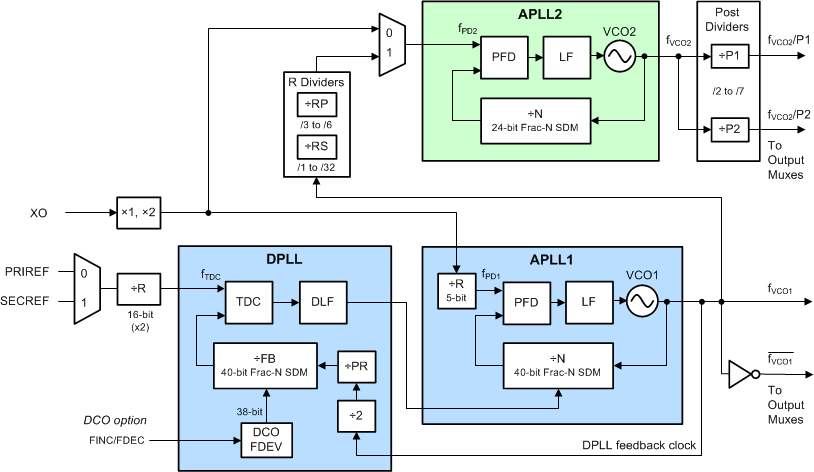
7.2.1 PLL Architecture Overview
Figure 7-2 shows the PLL architecture implemented in the LMK05318B-Q1. The primary "PLL1" channel consists of a digital PLL (DPLL) and analog PLL (APLL1) with integrated BAW VCO (VCO1) capable of generating clocks with RMS phase jitter of 50fs typical. A secondary APLL (APLL2) with integrated LC VCO (VCO2) can be used as an additional clock generation domain with RMS phase jitter of 130fs typical.
The DPLL is comprised of a time-to-digital converter (TDC), digital loop filter (DLF), and 40-bit fractional feedback (FB) divider with sigma-delta-modulator (SDM). The APLLs are comprised of a reference (R) divider, phase-frequency detector (PFD), loop filter (LF), fractional feedback (N) divider with SDM, and VCO. APLL2 has a reference selection mux that allows APLL2 to be either locked to the VCO domain of the APLL1 (Cascaded APLL2) or locked to the XO input (Non-Cascaded APLL2). Otherwise, APLL2 can be disabled (powered-down) if this clock domain is not needed. The VCO of the APLL1 feeds the output clock distribution blocks directly, whereas the VCO of the APLL2 drives the clock distribution blocks through the VCO post-dividers.

The following sections describe the basic principle of operation for DPLL mode and APLL-only mode. See PLL Operating Modes for more details on the PLL modes of operation including holdover.