JAJSKW2B June 2020 – June 2021 LMK05318B
PRODUCTION DATA
- 1 特長
- 2 アプリケーション
- 3 概要
- 4 Revision History
- 5 概要 (続き)
- 6 Pin Configuration and Functions
- 7 Specifications
- 8 Parameter Measurement Information
-
9 Detailed Description
- 9.1 Overview
- 9.2 Functional Block Diagram
- 9.3
Feature Description
- 9.3.1 Oscillator Input (XO_P/N)
- 9.3.2 Reference Inputs (PRIREF_P/N and SECREF_P/N)
- 9.3.3 Clock Input Interfacing and Termination
- 9.3.4 Reference Input Mux Selection
- 9.3.5 Hitless Switching
- 9.3.6 Gapped Clock Support on Reference Inputs
- 9.3.7 Input Clock and PLL Monitoring, Status, and Interrupts
- 9.3.8
PLL Relationships
- 9.3.8.1 PLL Frequency Relationships
- 9.3.8.2 Analog PLLs (APLL1, APLL2)
- 9.3.8.3 APLL Reference Paths
- 9.3.8.4 APLL Phase Frequency Detector (PFD) and Charge Pump
- 9.3.8.5 APLL Feedback Divider Paths
- 9.3.8.6 APLL Loop Filters (LF1, LF2)
- 9.3.8.7 APLL Voltage Controlled Oscillators (VCO1, VCO2)
- 9.3.8.8 APLL VCO Clock Distribution Paths (P1, P2)
- 9.3.8.9 DPLL Reference (R) Divider Paths
- 9.3.8.10 DPLL Time-to-Digital Converter (TDC)
- 9.3.8.11 DPLL Loop Filter (DLF)
- 9.3.8.12 DPLL Feedback (FB) Divider Path
- 9.3.9 Output Clock Distribution
- 9.3.10 Output Channel Muxes
- 9.3.11 Output Dividers (OD)
- 9.3.12 Clock Outputs (OUTx_P/N)
- 9.3.13 Glitchless Output Clock Start-Up
- 9.3.14 Clock Output Interfacing and Termination
- 9.3.15 Output Synchronization (SYNC)
- 9.3.16 Zero-Delay Mode (ZDM) Synchronization for 1-PPS Input and Output
- 9.4 Device Functional Modes
- 9.5 Programming
- 10Application and Implementation
- 11Power Supply Recommendations
- 12Layout
- 13Device and Documentation Support
- 14Mechanical, Packaging, and Orderable Information
パッケージ・オプション
メカニカル・データ(パッケージ|ピン)
- RGZ|48
サーマルパッド・メカニカル・データ
- RGZ|48
発注情報
9.5.1 Interface and Control
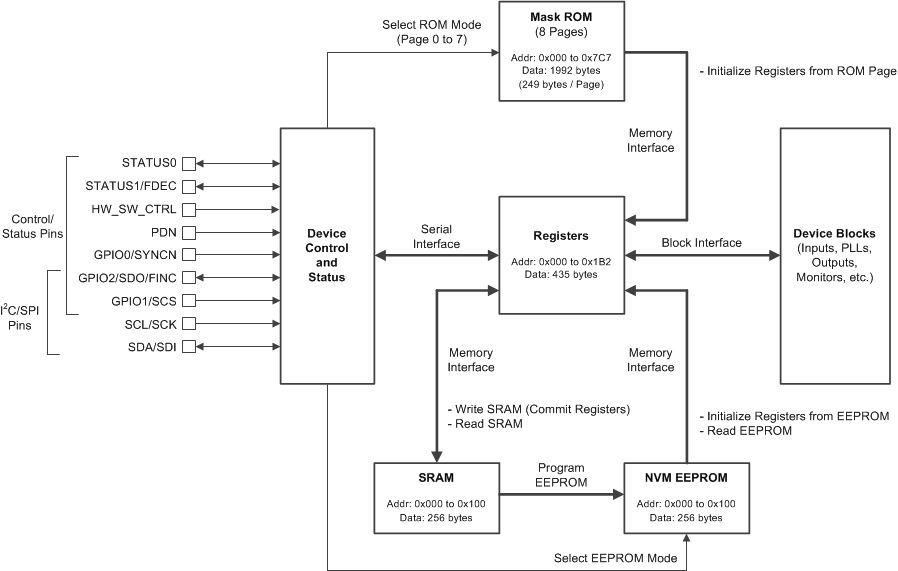
A system host device (MCU or FPGA) can use either I2C or SPI to access the register, SRAM, and EEPROM maps. The register and EEPROM map configurations are the same for I2C and SPI. The device can be initialized, controlled, and monitored through register access during normal operation (when PDN is deasserted). Some device features can also be controlled and monitored through the external logic control and status pins.
In the absence of a host, the LMK05318B can self-start from its on-chip EEPROM or ROM page depending on the state of HW_SW_CTRL pin. The EEPROM or ROM page is used to initialize the registers upon device POR. A custom EEPROM configuration can be programmed in-system through the register interface by either I2C or SPI. The ROM configurations are fixed in hardware and cannot be modified.
Figure 9-36 shows the device control pin, register, and memory interfaces. The arrows refer to the control interface directions between the different blocks.
The register map has 435 data bytes. Some registers, such as status registers and internal test/diagnostic registers (above R352), do not need to be written during device initialization.
The SRAM/EEPROM map has one register page with 256 data bytes. The SRAM/EEPROM map has fewer bytes because not all bit fields are mapped from the register space. To program the EEPROM, it is necessary to write the register contents to SRAM (internal register commit or direct write), then Program EEPROM with the register contents from SRAM.
The ROM map has eight register pages with 249 data bytes per page. The ROM contents are fixed in hardware and cannot be modified.
 Figure 9-36 Device Control, Register, and Memory Interfaces