JAJSIA5D December 2019 – February 2022 LMK1C1102 , LMK1C1103 , LMK1C1104
PRODUCTION DATA
- 1 特長
- 2 アプリケーション
- 3 概要
- 4 Revision History
- 5 Device Comparison
- 6 Pin Configuration and Functions
- 7 Specifications
- 8 Parameter Measurement Information
- 9 Detailed Description
- 10Application and Implementation
- 11Power Supply Recommendations
- 12Layout
- 13Device and Documentation Support
- 14Mechanical, Packaging, and Orderable Information
パッケージ・オプション
メカニカル・データ(パッケージ|ピン)
サーマルパッド・メカニカル・データ
発注情報
6 Pin Configuration and Functions
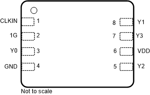
Figure 6-1 LMK1C1102 PW Package8-Pin TSSOPTop View
Figure 6-3 LMK1C1103 PW Package8-Pin TSSOPTop View

- The DQF (WSON) package is equivalent to the DFN package of other vendors.
- The DQF (WSON) package is equivalent to the DFN package of other vendors.
Figure 6-4 LMK1C1104 PW Package8-Pin TSSOPTop View
Table 6-1 Pin Functions
| PIN | TYPE | DESCRIPTION | |||
|---|---|---|---|---|---|
| NAME | LMK1C 1102 |
LMK1C 1103 |
LMK1C 1104 |
||
| LVCMOS CLOCK INPUT | |||||
| CLKIN | 1 | 1 | 1 | Input | Single-ended clock input with internal 300-kΩ (typical) pulldown resistor to GND. Typically connected to a single-ended clock input. |
| CLOCK OUTPUT ENABLE | |||||
| 1G | 2 | 2 | 2 | Input | Global Output Enable with internal 300-kΩ (typical) pulldown
resistor to GND. Typically connected to VDD with external pullup
resistor. HIGH: outputs enabled LOW: outputs disabled |
| LVCMOS CLOCK OUTPUT | |||||
| Y0 | 3 | 3 | 3 | Output | LVCMOS output. Typically connected to a receiver. Unused outputs can be left floating. |
| Y1 | 8 | 8 | 8 | ||
| Y2 | — | 5 | 5 | ||
| Y3 | — | — | 7 | ||
| SUPPLY VOLTAGE | |||||
| VDD | 6 | 6 | 6 | Power | Power supply terminal. Typically connected to a 3.3-V, 2.5-V, or 1.8-V supply. The VDD pin is typically connected to an external 0.1-μF capacitor near the pin. |
| GROUND | |||||
| GND | 4 | 4 | 4 | GND | Power supply ground. |