SNAS888A September 2024 – November 2024 LMK1D2102L , LMK1D2106L
PRODUCTION DATA
- 1
- 1 Features
- 2 Applications
- 3 Description
- 4 Device Comparison
- 5 Pin Configuration and Functions
- 6 Specifications
- 7 Parameter Measurement Information
- 8 Detailed Description
- 9 Application and Implementation
- 10Device and Documentation Support
- 11Revision History
- 12Mechanical, Packaging, and Orderable Information
パッケージ・オプション
デバイスごとのパッケージ図は、PDF版データシートをご参照ください。
メカニカル・データ(パッケージ|ピン)
- RHA|40
サーマルパッド・メカニカル・データ
発注情報
6.6 Typical Characteristics
LMK1D210xL buffer typical characteristics are shown for current consumption, phase noise performance and timing diagrams and output common mode operation.
Note that these graphs serve as a guidance to the users on what to expect for the range of operating frequency supported by the LMK1D210xL. These graphs are plotted for a limited number of frequencies and load conditions, which do not represent the customer system.
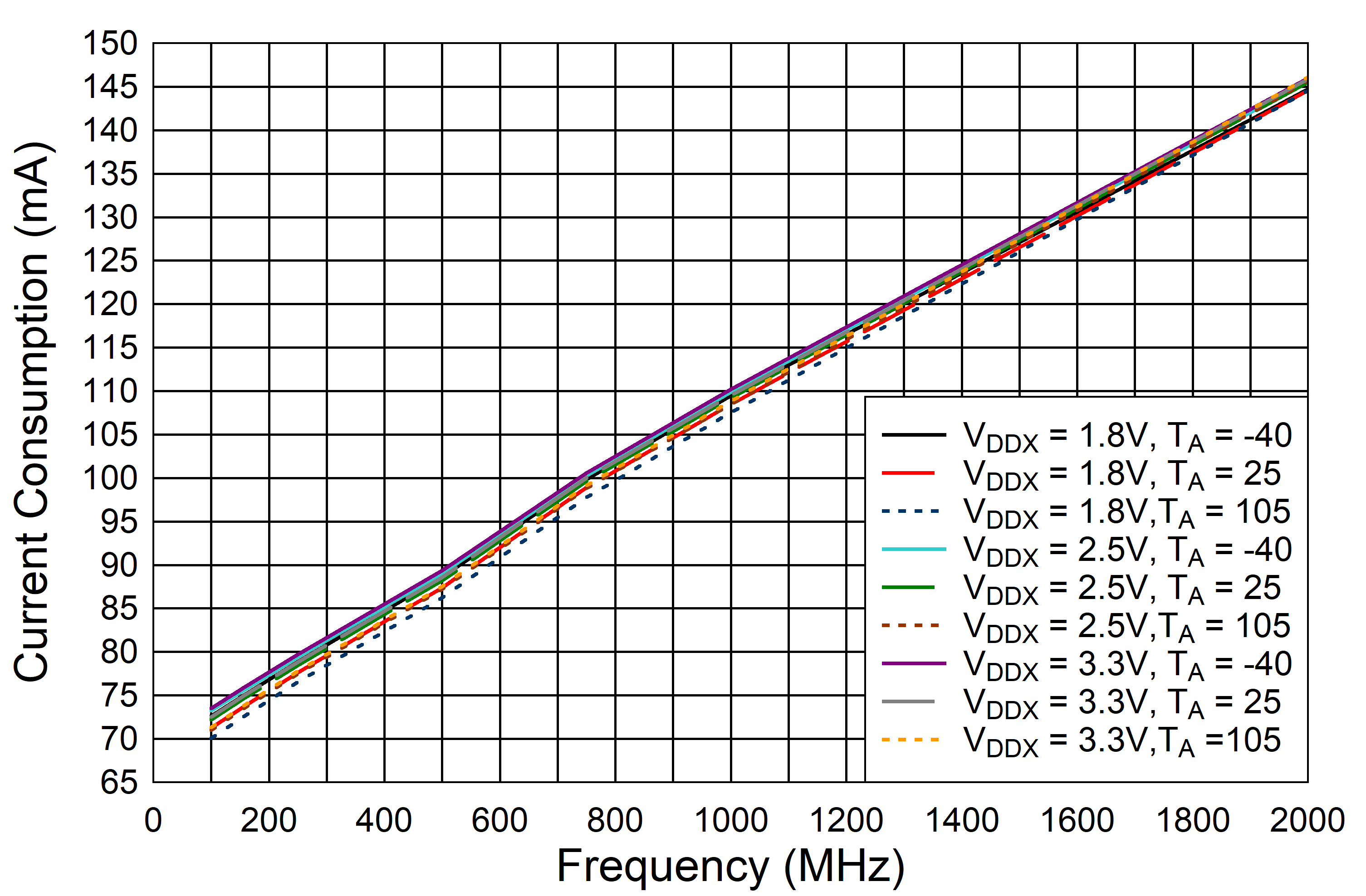 Figure 6-1 LMK1D2102L Current Consumption vs.
Frequency, AMP_SELA = 0
Figure 6-3 LMK1D2104L Current Consumption vs. Frequency, AMP_SELA = 0
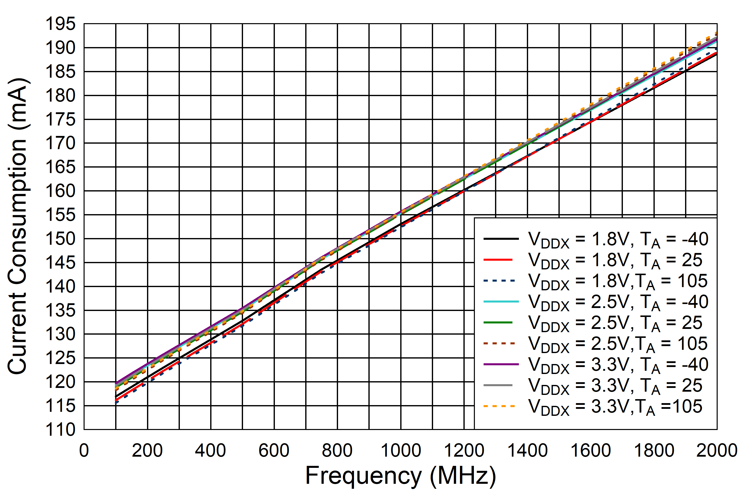 Figure 6-5 LMK1D2106L Current
Consumption vs. Frequency, AMP_SELA and AMP_SELB = 0
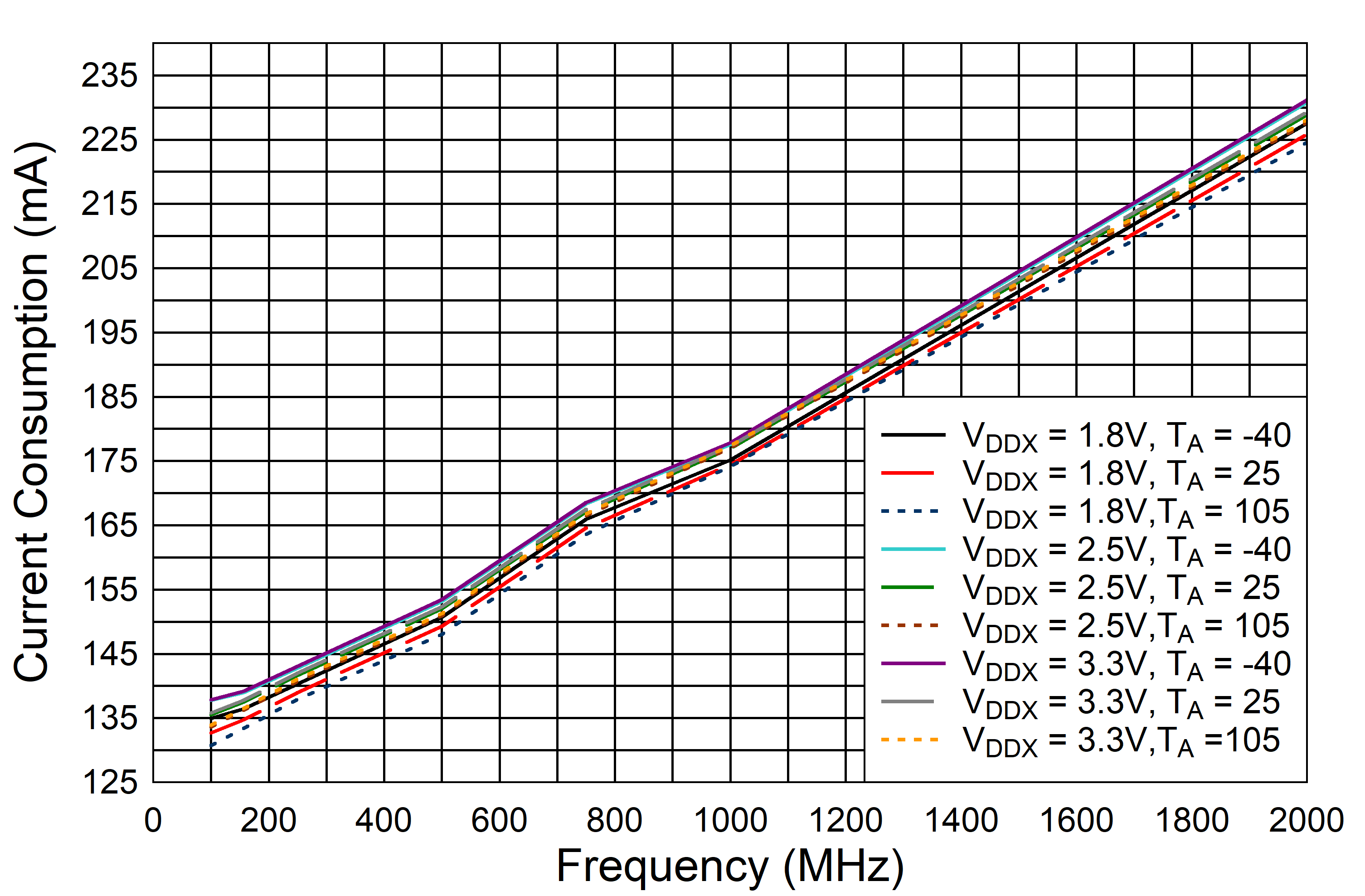 Figure 6-7 LMK1D2108L Current
Consumption vs. Frequency, AMP_SELA and AMP_SELB = 0
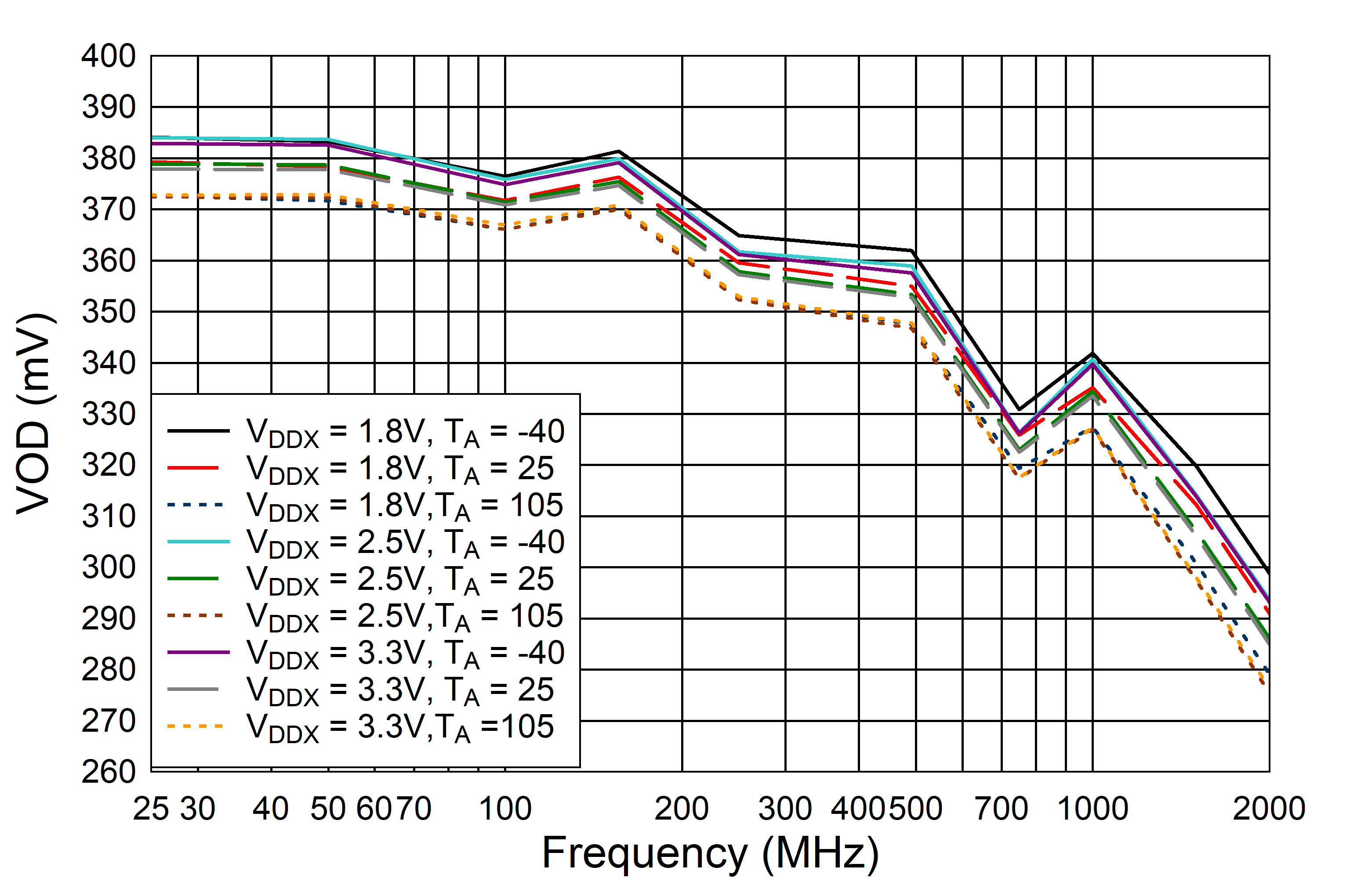 Figure 6-9 LMK1D210xL VOD vs.
Frequency, AMP_SELA / AMP_SELB = 0
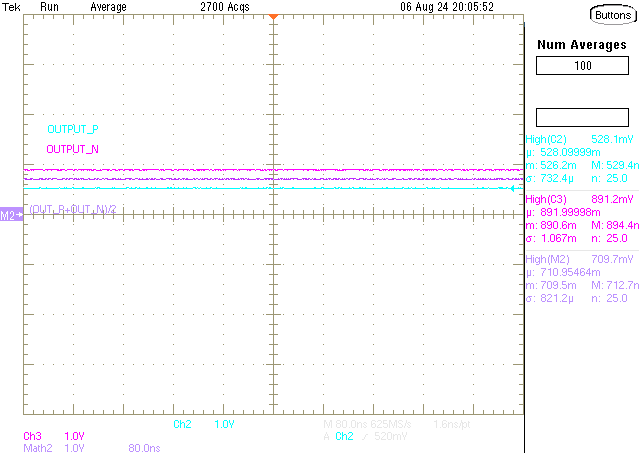 Figure 6-11 LMK1D210xL DC Output Common Mode at 1.8V
Supply Condition, Differential Low (AMP_SELA / AMP_SELB = 0)
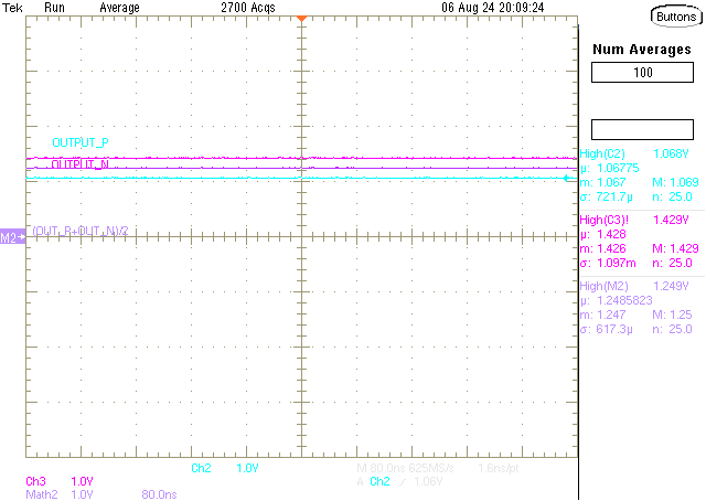 Figure 6-13 LMK1D210xL DC Output Common Mode at
2.5V/3.3V Supply Condition, Differential Low (AMP_SELA / AMP_SELB = 0)
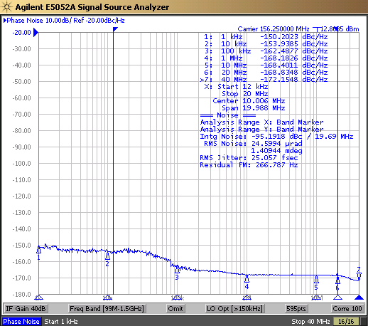 Figure 6-15 Input Source at 156.25MHz (12kHz - 20MHz)
 Figure 6-17 Input Source at 625MHz (12kHz -
20MHz)
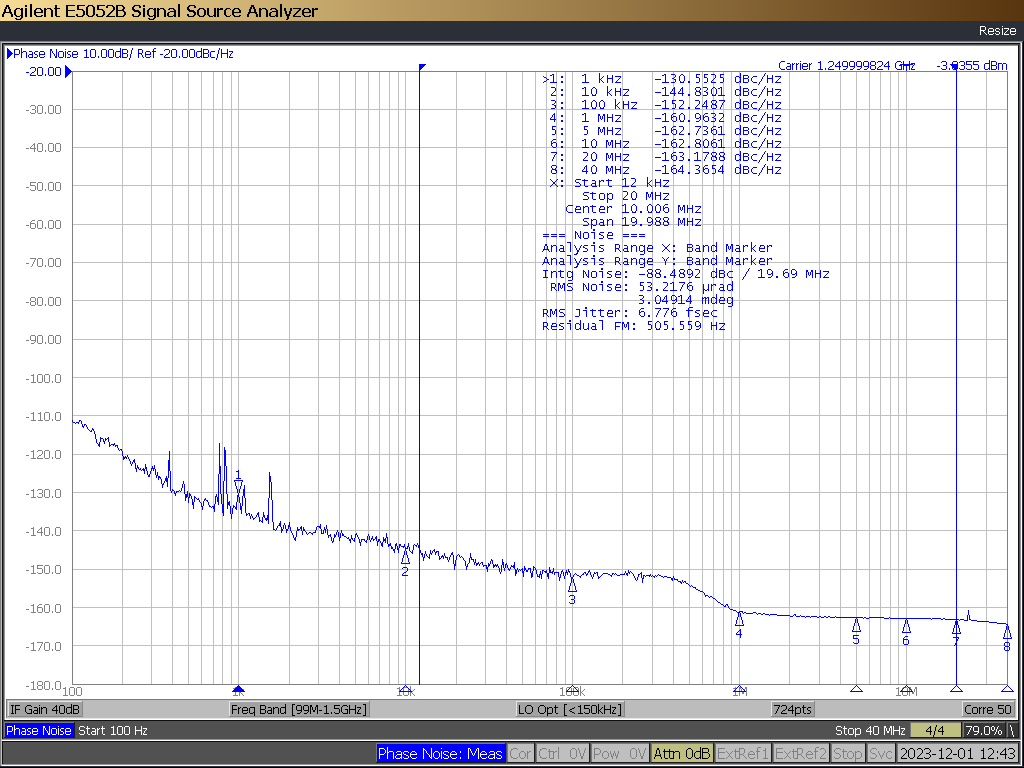 Figure 6-19 Input Source at 1250MHz (12kHz -
20MHz)
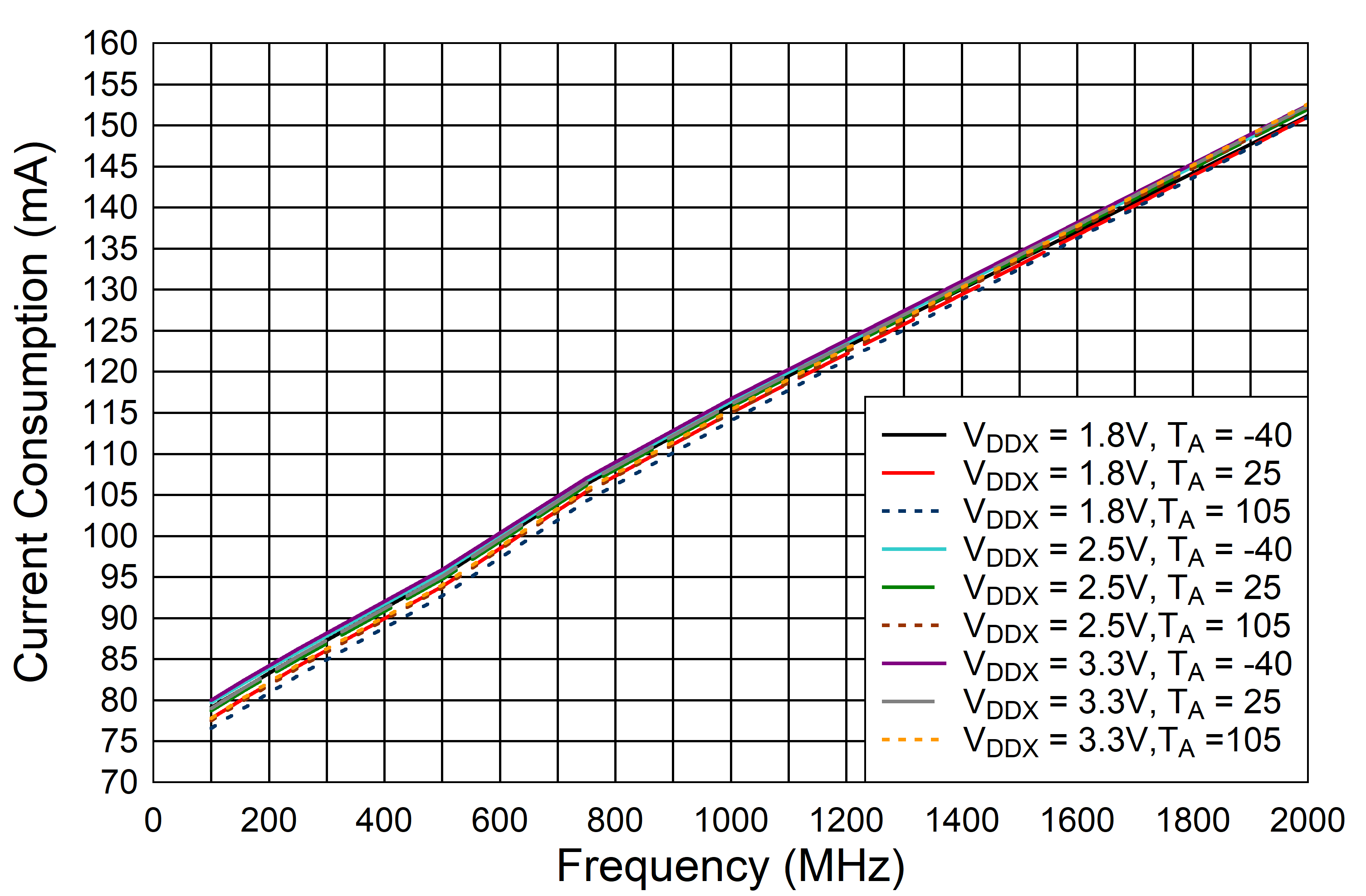 Figure 6-2 LMK1D2102L Current Consumption vs.
Frequency, AMP_SELA = Floating
 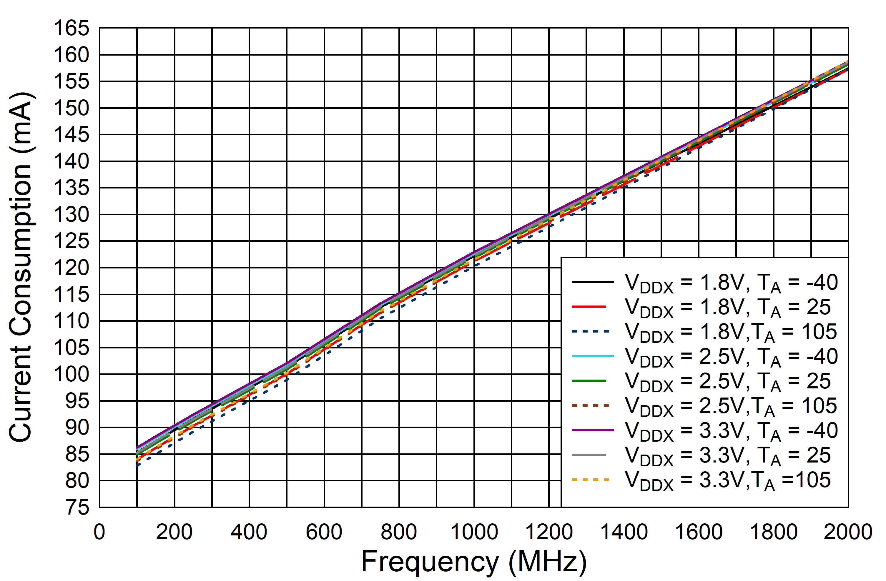 Figure 6-4 LMK1D2104L Current Consumption vs.
Frequency, AMP_SELA = Floating
 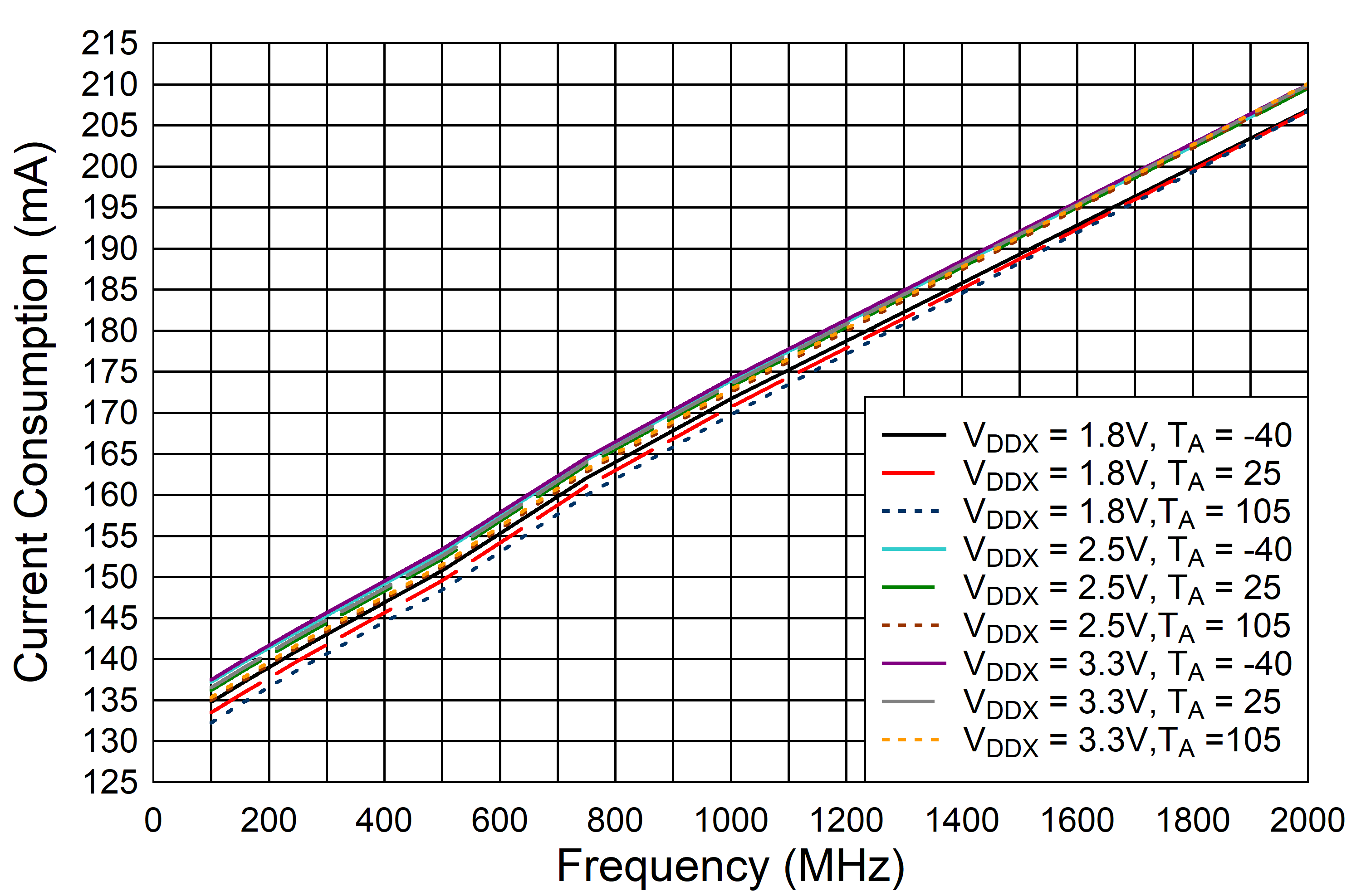 Figure 6-6 LMK1D2106L Current
Consumption vs. Frequency, AMP_SELA and AMP_SELB = Floating
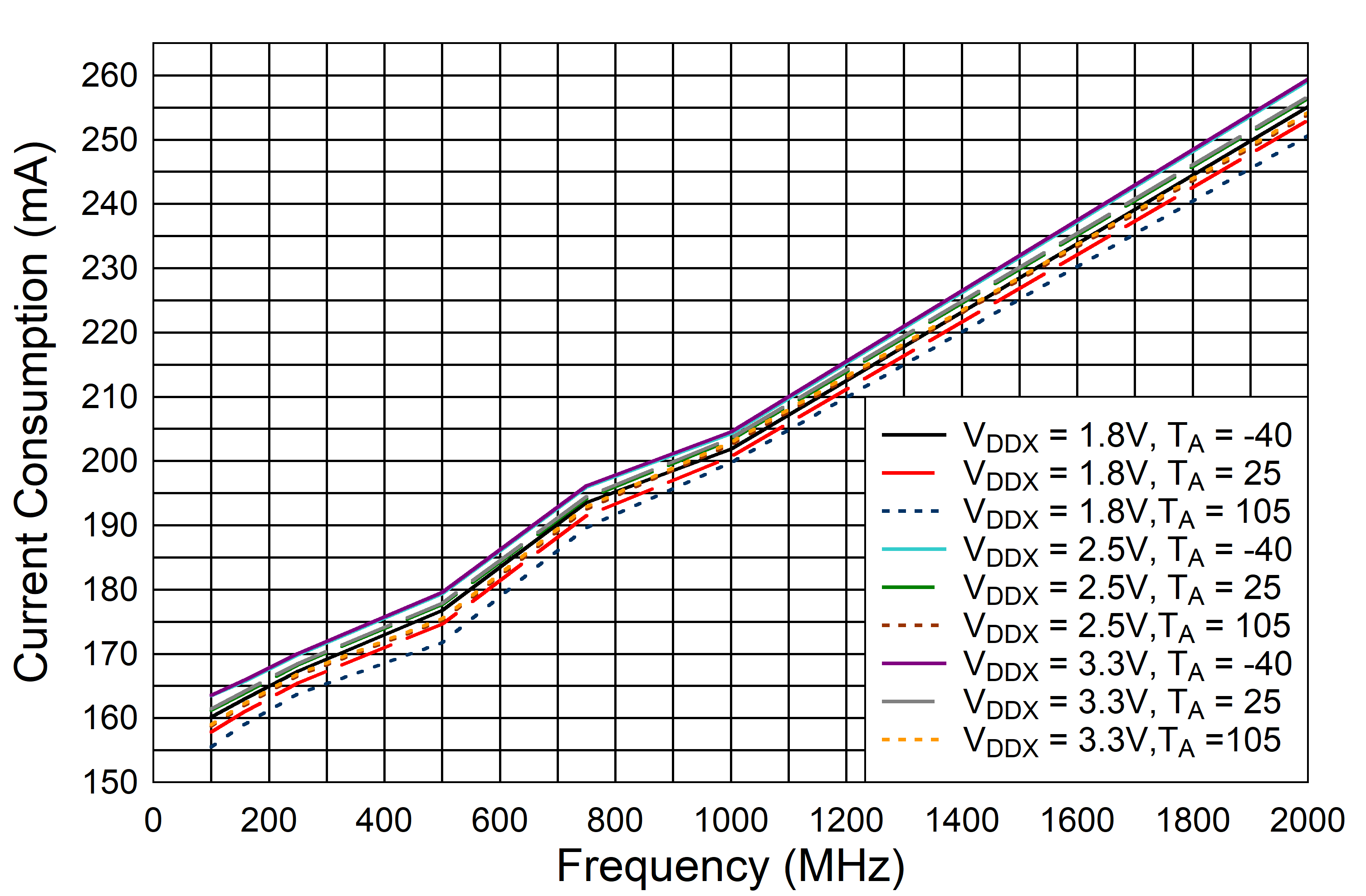 Figure 6-8 LMK1D2108L Current
Consumption vs. Frequency, AMP_SELA and AMP_SELB = Floating
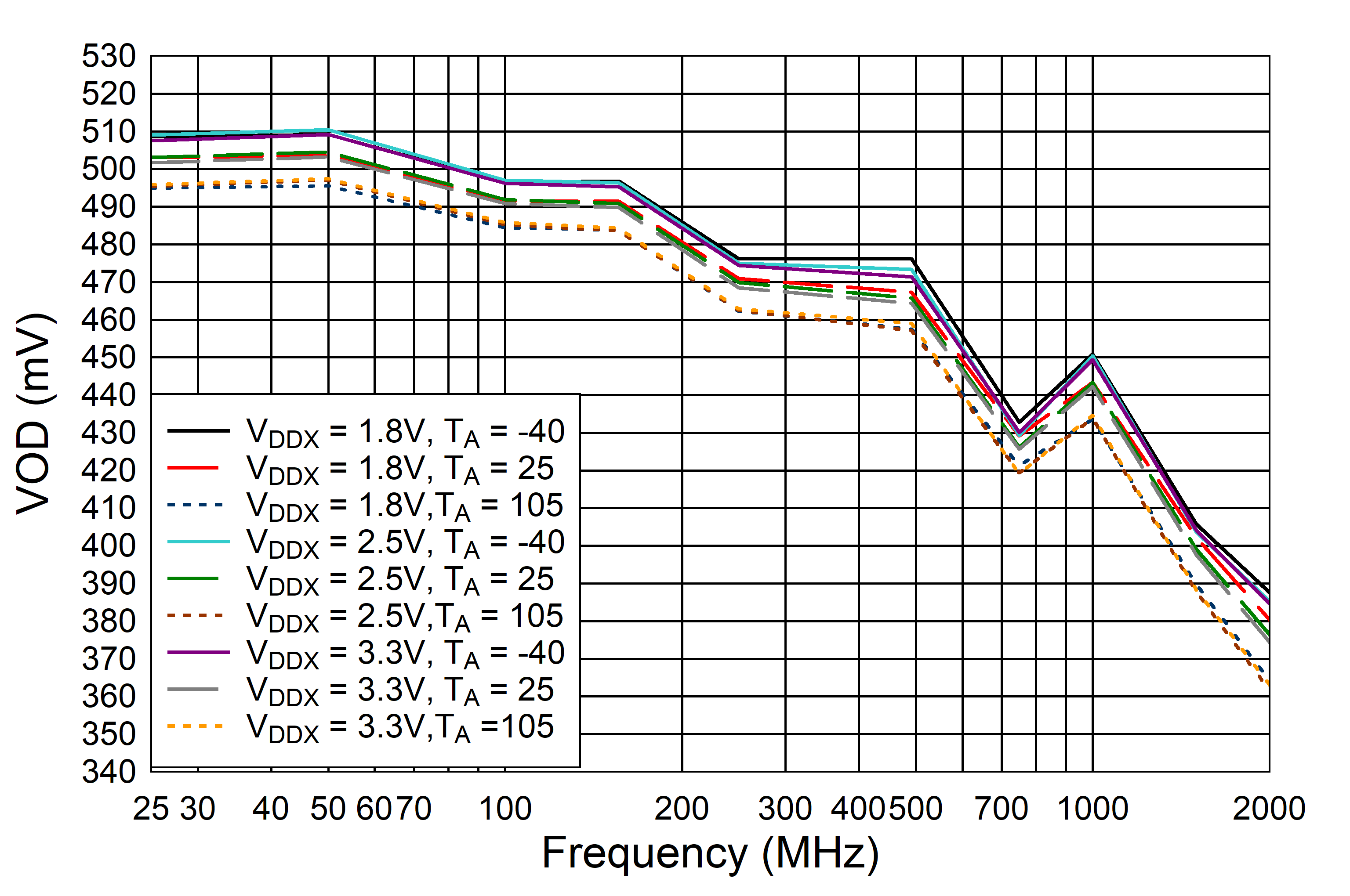 Figure 6-10 LMK1D210xL VOD vs. Frequency, AMP_SELA /
AMP_SELB = Floating
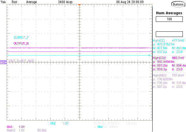 Figure 6-12 LMK1D210xL DC Output Common Mode at 1.8V
Supply Condition, Differential Low (AMP_SELA / AMP_SELB = Float)
 Figure 6-14 LMK1D210xL DC Output Common Mode at
2.5V/3.3V Supply Condition, Differential Low (AMP_SELA / AMP_SELB = Float)
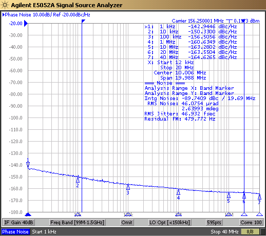
| See Note 1 and 2 in Graph Notes table | ||
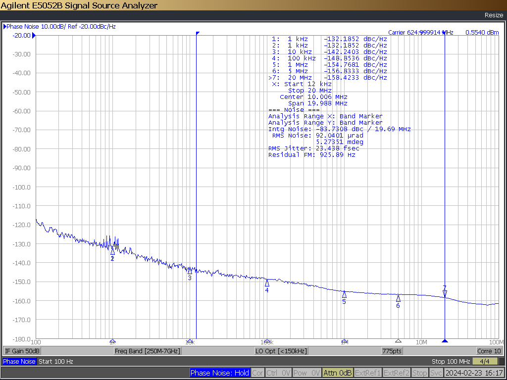
| See Note 1 and 3 in Graph Notes table | ||
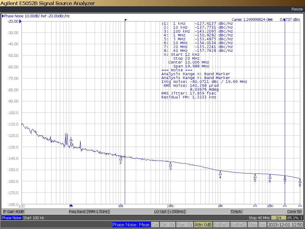
| See Note 1 and 4 in Graph Notes table | ||
Table 6-1 Graph Notes
| NOTE | ||||
|---|---|---|---|---|
| (1) | The typical RMS jitter values in the plots show the total output RMS jitter (JOUT) for each frequency and the source clock RMS jitter (JSOURCE). From these values, the Additive RMS Jitter can be calculated as: JADD = SQRT(JOUT2 – JSOURCE2). | |||
| (2) | JADD at 156.25MHz = SQRT(46.9322- 25.0572) = 39.68fs. | |||
| (3) | JADD at 625MHz = SQRT(23.4382- 8.4332) = 21.87fs. | |||
| (4) | JADD at 1250MHz = SQRT(17.8592- 6.7762) = 16.52fs. | |||