JAJSP85 December 2023 LMK5C33216A
PRODUCTION DATA
- 1
- 1 特長
- 2 アプリケーション
- 3 概要
- 4 Pin Configuration and Functions
- 5 Specifications
- 6 Parameter Measurement Information
-
7 Detailed Description
- 7.1 Overview
- 7.2 Functional Block Diagram
- 7.3
Feature Description
- 7.3.1 Oscillator Input (XO)
- 7.3.2 Reference Inputs
- 7.3.3 Clock Input Interfacing and Termination
- 7.3.4 Reference Input Mux Selection
- 7.3.5 Hitless Switching
- 7.3.6 Gapped Clock Support on Reference Inputs
- 7.3.7 Input Clock and PLL Monitoring, Status, and Interrupts
- 7.3.8
PLL Relationships
- 7.3.8.1 PLL Frequency Relationships
- 7.3.8.2 Analog PLLs (APLL1, APLL2, APLL3)
- 7.3.8.3 APLL Reference Paths
- 7.3.8.4 APLL Phase Frequency Detector (PFD) and Charge Pump
- 7.3.8.5 APLL Feedback Divider Paths
- 7.3.8.6 APLL Loop Filters (LF1, LF2, LF3)
- 7.3.8.7 APLL Voltage-Controlled Oscillators (VCO1, VCO2, VCO3)
- 7.3.8.8 APLL VCO Clock Distribution Paths
- 7.3.8.9 DPLL Reference (R) Divider Paths
- 7.3.8.10 DPLL Time-to-Digital Converter (TDC)
- 7.3.8.11 DPLL Loop Filter (DLF)
- 7.3.8.12 DPLL Feedback (FB) Divider Path
- 7.3.9 Output Clock Distribution
- 7.3.10 Output Channel Muxes
- 7.3.11 Output Dividers (OD)
- 7.3.12 SYSREF/1-PPS
- 7.3.13 Output Delay
- 7.3.14 Clock Outputs (OUTx_P/N)
- 7.3.15 Glitchless Output Clock Start-Up
- 7.3.16 Clock Output Interfacing and Termination
- 7.3.17 Output Synchronization (SYNC)
- 7.3.18 Zero-Delay Mode (ZDM)
- 7.3.19 Time Elapsed Counter (TEC)
- 7.4 Device Functional Modes
- 7.5 Programming
-
8 Application and Implementation
- 8.1 Application Information
- 8.2 Typical Application
- 8.3 Best Design Practices
- 8.4 Power Supply Recommendations
- 8.5 Layout
- 9 Device and Documentation Support
- 10Revision History
- 11Mechanical, Packaging, and Orderable Information
7.3.3 Clock Input Interfacing and Termination
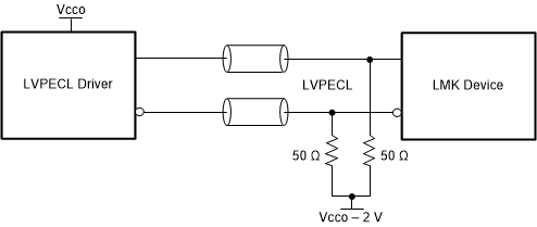
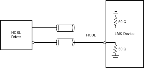
Figure 7-10 through Figure 7-13 show the recommended input interfacing and termination circuits. Unused clock inputs can be left floating or pulled down.
 Figure 7-10 Single-Ended LVCMOS (1.8 V, 2.5 V, 3.3 V) to Reference (INx_P) or XO Input (XO)
 Figure 7-11 DC-Coupled LVPECL to Reference (INx)
 Figure 7-12 DC-Coupled HSDS/LVDS to Reference (INx)
 Figure 7-13 HCSL (Load Terminated) to Reference (INx)