JAJSCC0C June 2016 – November 2017 LMK60A0-148351 , LMK60A0-148M , LMK60E0-156257 , LMK60E2-150M
PRODUCTION DATA.
- 1 特長
- 2 アプリケーション
- 3 概要
- 4 改訂履歴
- 5 Pin Configuration and Functions
-
6 Specifications
- 6.1 Absolute Maximum Ratings
- 6.2 ESD Ratings
- 6.3 Recommended Operating Conditions
- 6.4 Thermal Information
- 6.5 Electrical Characteristics - Power Supply
- 6.6 LVPECL Output Characteristics
- 6.7 LVDS Output Characteristics
- 6.8 HCSL Output Characteristics
- 6.9 OE Input Characteristics
- 6.10 Frequency Tolerance Characteristics
- 6.11 Power-On/Reset Characteristics (VDD)
- 6.12 PSRR Characteristics
- 6.13 PLL Clock Output Jitter Characteristics
- 6.14 Additional Reliability and Qualification
- 6.15 Typical Characteristics
- 7 Parameter Measurement Information
- 8 Power Supply Recommendations
- 9 Layout
- 10デバイスおよびドキュメントのサポート
- 11メカニカル、パッケージ、および注文情報
パッケージ・オプション
デバイスごとのパッケージ図は、PDF版データシートをご参照ください。
メカニカル・データ(パッケージ|ピン)
- SIA|6
サーマルパッド・メカニカル・データ
発注情報
6 Specifications
6.1 Absolute Maximum Ratings
over operating free-air temperature range (unless otherwise noted)(1)| MIN | MAX | UNIT | ||
|---|---|---|---|---|
| VDD | Device supply voltage | –0.3 | 3.6 | V |
| VIN | Output voltage for logic inputs | –0.3 | VDD + 0.3 | V |
| VOUT | Output voltage for clock outputs | –0.3 | VDD + 0.3 | V |
| TJ | Junction temperature | 150 | °C | |
| TSTG | Storage temperature | –40 | 125 | °C |
(1) Stresses beyond those listed under Absolute Maximum Ratings may cause permanent damage to the device. These are stress ratings only, which do not imply functional operation of the device at these or any other conditions beyond those indicated under Recommended Operating Conditions. Exposure to absolute maximum-rated conditions for extended periods may affect device reliability.
6.2 ESD Ratings
| VALUE | UNIT | |||
|---|---|---|---|---|
| V(ESD) | Electrostatic discharge | Human-body model (HBM), per ANSI/ESDA/JEDEC JS-001(1) | ±2000 | V |
| Charged-device model (CDM), per JEDEC specification JESD22-C101(2) | ±500 | |||
(1) JEDEC document JEP155 states that 500 V HBM allows safe manufacturing with a standard ESD control process.
(2) JEDEC document JEP157 states that 250 V CDM allows safe manufacturing with a standard ESD control process.
6.3 Recommended Operating Conditions
over operating free-air temperature range (unless otherwise noted)| MIN | NOM | MAX | UNIT | ||
|---|---|---|---|---|---|
| VDD | Device supply voltage | 3.135 | 3.3 | 3.465 | V |
| TA | Ambient temperature | –40 | 25 | 85 | °C |
| TJ | Junction temperature | 120 | °C | ||
| tRAMP | VDD power-up ramp time | 0.1 | 100 | ms | |
6.4 Thermal Information
| THERMAL METRIC(1) | LMK60XX (2) (3) (4) | UNIT | |||
|---|---|---|---|---|---|
| SIA (QFM) | |||||
| 6 PINS | |||||
| Airflow (LFM) 0 | Airflow (LFM) 200 | Airflow (LFM) 400 | |||
| RθJA | Junction-to-ambient thermal resistance | 55.2 | 46.4 | 43.7 | °C/W |
| RθJC(top) | Junction-to-case (top) thermal resistance | 34.6 | n/a | n/a | °C/W |
| RθJB | Junction-to-board thermal resistance | 37.7 | n/a | n/a | °C/W |
| ψJT | Junction-to-top characterization parameter | 11.3 | 17.6 | 22.5 | °C/W |
| ψJB | Junction-to-board characterization parameter | 37.7 | 41.5 | 40.1 | °C/W |
| RθJC(bot) | Junction-to-case (bottom) thermal resistance | n/a | n/a | n/a | °C/W |
(1) For more information about traditional and new thermal metrics, see the Semiconductor and IC Package Thermal Metrics application report.
(2) The package thermal resistance is calculated on a 4 layer JEDEC board.
(3) Connected to GND with 3 thermal vias (0.3-mm diameter).
(4) ψJB (junction to board) is used when the main heat flow is from the junction to the GND pad. See the Layout Guidelines section for more information on ensuring good system reliability and quality.
6.5 Electrical Characteristics - Power Supply(1)
VDD = 3.3 V ± 5%, TA = -40C to 85°C| PARAMETER | TEST CONDITIONS | MIN | TYP | MAX | UNIT | |
|---|---|---|---|---|---|---|
| IDD | Device current consumption | LVPECL(2) | 162 | 208 | mA | |
| LVDS | 152 | 196 | ||||
| HCSL | 155 | 196 | ||||
| IDD-PD | Device current consumption when output is disabled | OE = GND | 136 | mA | ||
(1) Refer to Parameter Measurement Information for relevant test conditions.
(2) On-chip power dissipation should exclude 40 mW, dissipated in the 150 Ω termination resistors, from total power dissipation.
6.6 LVPECL Output Characteristics(1)
VDD = 3.3 V ± 5%, TA = -40C to 85°C| PARAMETER | TEST CONDITIONS | MIN | TYP | MAX | UNIT | |
|---|---|---|---|---|---|---|
| fOUT | Output frequency(2) | 10 | 800 | MHz | ||
| VOD | Output voltage swing (VOH – VOL)(2) | 700 | 800 | 1200 | mV | |
| VOUT, DIFF, PP | Differential output peak-to-peak swing | 2 × |VOD| | V | |||
| VOS | Output common-mode voltage | VDD – 1.55 | V | |||
| tR / tF | Output rise/fall time (20% to 80%)(3) | 150 | 250 | ps | ||
| ODC | Output duty cycle(3) | 45% | 55% | |||
(1) Refer to Parameter Measurement Information for relevant test conditions.
(2) An output frequency over fOUT max spec is possible, but output swing may be less than VOD min spec.
(3) Ensured by characterization.
6.7 LVDS Output Characteristics(1)
VDD = 3.3 V ± 5%, TA = -40°C to 85°C| PARAMETER | TEST CONDITIONS | MIN | TYP | MAX | UNIT | |
|---|---|---|---|---|---|---|
| fOUT | Output frequency(1) | 10 | 800 | MHz | ||
| VOD | Output voltage swing (VOH - VOL)(1) |
300 | 390 | 480 | mV | |
| VOUT, DIFF, PP | Differential output peak-to-peak swing | 2 × |VOD| | V | |||
| VOS | Output common-mode voltage | 1.2 | V | |||
| tR / tF | Output rise/fall time (20% to 80%)(2) | 150 | 250 | ps | ||
| ODC | Output duty cycle(2) | 45% | 55% | |||
| ROUT | Differential output impedance | 125 | Ω | |||
(1) An output frequency over fOUT max spec is possible, but output swing may be less than VOD min spec.
(2) Ensured by characterization.
6.8 HCSL Output Characteristics(1)
VDD = 3.3 V ± 5%, TA = -40°C to 85°C| PARAMETER | TEST CONDITIONS | MIN | TYP | MAX | UNIT | |
|---|---|---|---|---|---|---|
| fOUT | Output frequency | 10 | 400 | MHz | ||
| VOH | Output high voltage | 600 | 850 | mV | ||
| VOL | Output low voltage | –100 | 100 | mV | ||
| VCROSS | Absolute crossing voltage(2)(3) | 250 | 475 | mV | ||
| VCROSS-DELTA | Variation of VCROSS(2)(3) | 0 | 140 | mV | ||
| dV/dt | Slew rate(4) | 0.8 | 2 | V/ns | ||
| ODC | Output duty cycle(4) | 45% | 55% | |||
(1) Refer to Parameter Measurement Information for relevant test conditions.
(2) Measured from -150 mV to +150 mV on the differential waveform with the 300 mVpp measurement window centered on the differential zero crossing.
(3) Ensured by design.
(4) Ensured by characterization.
6.9 OE Input Characteristics
VDD = 3.3 V ± 5%, TA = -40°C to 85°C| PARAMETER | TEST CONDITIONS | MIN | TYP | MAX | UNIT | |
|---|---|---|---|---|---|---|
| VIH | Input high voltage | 1.4 | V | |||
| VIL | Input low voltage | 0.6 | V | |||
| IIH | Input high current | VIH = VDD | –40 | 40 | µA | |
| IIL | Input low current | VIL = GND | –40 | 40 | µA | |
| CIN | Input capacitance | 2 | pF | |||
6.10 Frequency Tolerance Characteristics(1)
VDD = 3.3 V ± 5%, TA = -40°C to 85°C| PARAMETER | TEST CONDITIONS | MIN | TYP | MAX | UNIT | |
|---|---|---|---|---|---|---|
| fT | Total frequency tolerance | LMK60X2: All output formats, frequency bands and device junction temperature up to 125°C; includes initial freq tolerance, temperature & supply voltage variation, solder reflow and aging (10 years) | –50 | 50 | ppm | |
| LMK60X0: All output formats, frequency bands and device junction temperature up to 115°C; includes initial freq tolerance, temperature & supply voltage variation, solder reflow and aging (5 years at 40°C) | –25 | 25 | ppm | |||
(1) Ensured by characterization.
6.11 Power-On/Reset Characteristics (VDD)
VDD = 3.3 V ± 5%, TA = -40°C to 85°C| PARAMETER | TEST CONDITIONS | MIN | TYP | MAX | UNIT | |
|---|---|---|---|---|---|---|
| VTHRESH | Threshold voltage(1) | 2.72 | 2.95 | V | ||
| VDROOP | Allowable voltage droop(2) | 0.1 | V | |||
| tSTARTUP | Start-up time (1) | Time elapsed from VDD at 3.135 V to output enabled | 10 | ms | ||
| tOE-EN | Output enable time(2) | Time elapsed from OE at VIH to output enabled | 50 | µs | ||
| tOE-DIS | Output disable time(2) | Time elapsed from OE at VIL to output disabled | 50 | µs | ||
(1) Ensured by characterization.
(2) Ensured by design.
6.12 PSRR Characteristics(1)
VDD = 3.3 V, TA = 25°C, FS[1:0] = NC, NC| PARAMETER | TEST CONDITIONS | MIN | TYP | MAX | UNIT | |
|---|---|---|---|---|---|---|
| PSRR | Spurs induced by 50-mV power supply ripple(2)(3) at 156.25-MHz output, all output types | Sine wave at 50 kHz | –60 | dBc | ||
| Sine wave at 100 kHz | –60 | |||||
| Sine wave at 500 kHz | –60 | |||||
| Sine wave at 1 MHz | –60 | |||||
(1) Refer to Parameter Measurement Information for relevant test conditions.
(2) Measured max spur level with 50 mVpp sinusoidal signal between 50 kHz and 1 MHz applied on VDD pin
(3) DJSPUR (ps, pk-pk) = [2*10(SPUR/20) / (π*fOUT)]*1e6, where PSRR or SPUR in dBc and fOUT in MHz.
6.13 PLL Clock Output Jitter Characteristics(1)(3)
VDD = 3.3 V ± 5%, TA = -40°C to 85°C| PARAMETER | TEST CONDITIONS | MIN | TYP | MAX | UNIT | |
|---|---|---|---|---|---|---|
| RJ | RMS phase jitter(2)
(12 kHz – 20 MHz) |
fOUT ≥ 100 MHz, All output types | 150 | 250 | fs RMS | |
(1) Refer to Parameter Measurement Information for relevant test conditions.
(2) Ensured by characterization.
(3) Phase jitter measured with Agilent E5052 signal source analyzer using a differential-to-single ended converter (balun or buffer).
6.14 Additional Reliability and Qualification
| PARAMETER | CONDITION / TEST METHOD |
|---|---|
| Mechanical Shock | MIL-STD-202, Method 213 |
| Mechanical Vibration | MIL-STD-202, Method 204 |
| Moisture Sensitivity Level | J-STD-020, MSL3 |
6.15 Typical Characteristics
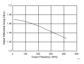
 Figure 1. LVPECL Differential Output Swing vs Frequency
 Figure 3. HCSL Differential Output Swing vs Frequency
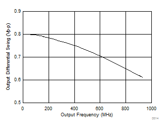
 Figure 2. LVDS Differential Output Swing vs Frequency