JAJSDN6C December 2016 – December 2017 LMK60E0-156M , LMK60E0-212M , LMK60E2-100M , LMK60E2-125M , LMK60E2-156M , LMK60I2-100M , LMK60I2-322M
PRODUCTION DATA.
- 1 特長
- 2 アプリケーション
- 3 概要
- 4 改訂履歴
- 5 Pin Configuration and Functions
-
6 Specifications
- 6.1 Absolute Maximum Ratings
- 6.2 ESD Ratings
- 6.3 Recommended Operating Conditions
- 6.4 Thermal Information
- 6.5 Electrical Characteristics - Power Supply
- 6.6 LVPECL Output Characteristics
- 6.7 LVDS Output Characteristics
- 6.8 HCSL Output Characteristics
- 6.9 OE Input Characteristics
- 6.10 Frequency Tolerance Characteristics
- 6.11 Power-On/Reset Characteristics (VDD)
- 6.12 PSRR Characteristics
- 6.13 PLL Clock Output Jitter Characteristics
- 6.14 Additional Reliability and Qualification
- 7 Parameter Measurement Information
- 8 Power Supply Recommendations
- 9 Layout
- 10デバイスおよびドキュメントのサポート
- 11メカニカル、パッケージ、および注文情報
パッケージ・オプション
デバイスごとのパッケージ図は、PDF版データシートをご参照ください。
メカニカル・データ(パッケージ|ピン)
- SIA|6
サーマルパッド・メカニカル・データ
発注情報
9 Layout
9.1 Layout Guidelines
The following sections provides recommendations for board layout, solder reflow profile, and power supply bypassing when using LMK60EX to ensure good thermal and electrical performance, along with overall signal integrity of entire system.
9.1.1 Ensuring Thermal Reliability
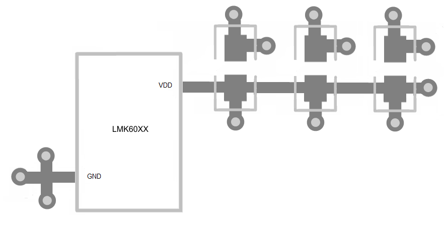
The LMK60EX is a high-performance device. Therefore, pay careful attention to device configuration and the printed-circuit board (PCB) layout with respect to power consumption. The ground pin must be connected to the ground plane of the PCB through three vias or more, as shown in Figure 9, to maximize thermal dissipation out of the package.
Equation 1 describes the relationship between the PCB temperature around the LMK60EX and its junction temperature.
where
- TB: PCB temperature around the LMK60EX
- TJ: Junction temperature of LMK60EX
- ΨJB: Junction-to-board thermal resistance parameter of LMK60EX (48.7°C/W without airflow)
- P: On-chip power dissipation of LMK60EX
To ensure that the maximum junction temperature of LMK60EX is below 105°C, it can be calculated that the maximum PCB temperature without airflow should be at 87°C or below when the device is optimized for best performance resulting in maximum on-chip power dissipation of 0.36 W.
9.1.2 Best Practices for Signal Integrity
For best electrical performance and signal integrity of entire system with LMK60EX, TI recommends routing vias into decoupling capacitors and then into the LMK60EX. TI also recommends increasing the via count and width of the traces wherever possible. These steps ensure lowest impedance and shortest path for high frequency current flow. Figure 9 shows the layout recommendation for LMK60EX.
 Figure 9. LMK60EX Layout Recommendation for Power Supply and Ground
9.1.3 Recommended Solder Reflow Profile
TI recommends following the recommendations of the solder paste supplier to optimize flux activity and to achieve proper melting temperatures of the alloy within the guidelines of J-STD-20. Processing the LMK60EX to be processed with the lowest peak temperature possible while also remaining below the components peak temperature rating as listed on the MSL label is preferred. The exact temperature profile would depend on several factors including maximum peak temperature for the component as rated on the MSL label, board thickness, PCB material type, PCB geometries, component locations, sizes, densities within PCB, as well as the recommended soldering profile from the manufacturer and capability of the reflow equipment to as confirmed by the SMT assembly operation.