JAJSKX8D December 2020 – October 2024 LMP7704-SP
PRODUCTION DATA
4 Pin Configuration and Functions
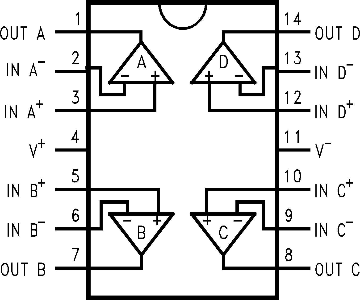
 Figure 4-1 HBH Package, 14-Pin CFP (Top
View)
Figure 4-1 HBH Package, 14-Pin CFP (Top
View)Table 4-1 Pin Functions
| PIN | TYPE | DESCRIPTION | |
|---|---|---|---|
| NAME | NO. | ||
| IN A+ | 3 | Input | Noninverting input for amplifier A |
| IN A– | 2 | Input | Inverting input for amplifier A |
| IN B+ | 5 | Input | Noninverting input for amplifier B |
| IN B– | 6 | Input | Inverting input for amplifier B |
| IN C+ | 10 | Input | Noninverting input for amplifier C |
| IN C– | 9 | Input | Inverting input for amplifier C |
| IN D+ | 12 | Input | Noninverting input for amplifier D |
| IN D– | 13 | Input | Inverting input for amplifier D |
| OUT A | 1 | Output | Output for amplifier A |
| OUT B | 7 | Output | Output for amplifier B |
| OUT C | 8 | Output | Output for amplifier C |
| OUT D | 14 | Output | Output for amplifier D |
| V+ | 4 | Power | Positive supply |
| V– | 11 | Power | Negative supply |
| PAD | — | — | Backside thermal pad, internally shorted to LID. Thermally connected to the device substrate, but electrically high-impedance to the substrate. Connect the pad to V– to reduce parasitic capacitance and leakage paths. |
| LID | — | — | Topside metal lid, internally shorted to PAD. |