SNOSB80C February 2011 – October 2015 LMP8350
PRODUCTION DATA.
8 Application and Implementation
NOTE
Information in the following applications sections is not part of the TI component specification, and TI does not warrant its accuracy or completeness. TI’s customers are responsible for determining suitability of components for their purposes. Customers should validate and test their design implementation to confirm system functionality.
8.1 Application Information
8.1.1 Fully-Differential Operation
The LMP8350 will perform best when used with split supplies and in a fully-differential configuration. See Figure 29 for recommend circuits.
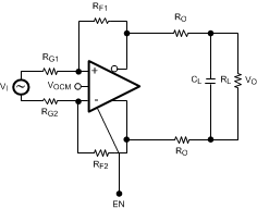 Figure 29. Typical Fully-Differential Application
The circuit shown in Figure 29 is a typical fully-differential application as might be used to drive a Sigma Delta ADC. In this circuit, closed-loop gain is calculated by Equation 1:
where
- RF=RF1=RF2 and RG=RG1=RG2
For all the applications in this data sheet , VIN is presumed to be the voltage presented to the circuit by the signal source. For differential signals this will be the difference of the signals on each input (which will be double the magnitude of each individual signal), while in single-ended inputs it will just be the driven input signal.
When fed with a differential signal, the LMP8350 provides excellent distortion, balance and common-mode rejection, provided the resistors RF, RG and any input termination resistors (RT) are well-matched and strict symmetry is observed in board layout. With a DC CMRR of over 80 dB, the DC and low frequency CMRR of most circuits will be dominated by the external resistor matching and board trace resistance. At low distortion levels, board layout symmetry and supply bypassing become a factor as well. It is assumed throughout this document that RF1 = RF2 and RG1 = RG2 for maximum channel symmetry
Precision resistors of at least 0.1% accuracy or better are recommended and careful board layout will also be required for optimum performance.
Operation with RF feedback resistors as low as 300 Ω is possible in the high and medium power modes. This will slightly improve the noise and bandwidth results. However, feedback resistors with RF values of less than 1 KΩ should be avoided in the low power mode due to the reduced output drive current capabilities. If low value resistors (< 300 Ω) must be used in the low power mode, the maximum output swing will need to be limited.
The resistors RO help keep the amplifier stable when presented with a load CL, as is common when driving an analog to digital converter (ADC).
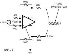 Figure 30. Fully-Differential Cable Driver
With up to 15 VPP differential output voltage swing and 80 mA of linear drive current, the LMP8350 makes an excellent precision cable driver as shown in Figure 30. The LMP8350 is also suitable for driving differential cables from a single-ended source.
8.1.2 Single Supply Operation
As shown in Figure 31, the input common-mode voltage is less than the output common voltage. It is set by current flowing through the feedback network from the device output. The input common-mode voltage range places constraints on gain settings. The input common-mode voltage is calculated in Equation 2. Possible solutions to this limitation include AC coupling the input signal, using split power supplies and limiting stage gain. AC coupling with single-supply is shown in Figure 32.
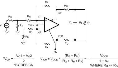 Figure 31. Relating AV to Input/Output Common-Mode Voltages
In Figure 31 the differential closed loop gain is = AV= RF/RG.
NOTE
In single-ended to differential operation VIN is measured single ended while VOUT is measured differentially. This means that gain is really one-half, or 6 dB, less when measured on either of the output pins separately.
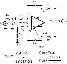 Figure 32. AC Coupled for Single-Supply Operation
8.1.3 Driving Analog to Digital Converters
Analog to digital converters (ADC) present challenging load conditions. They typically have high impedance inputs with large and often variable capacitive components. As well, there are usually current spikes associated with switched capacitor or sample and hold circuits. Figure 33 shows a typical circuit for driving an ADC. The two resistors serve to isolate the capacitive loading of the ADC from the amplifier and ensure stability. In addition, the resistors form part of a lowpass filter which helps to provide anti alias and noise reduction functions. The CS capacitor helps to smooth the current spikes associated with the internal switching circuits of the ADC and also are a key component in the lowpass filtering of the ADC input. The capacitor should be a low distortion capacitor, such as an NPO, to avoid causing significant distortion terms. In the circuit of Figure 33, the cutoff frequency of the filter is calculated by Equation 3. This should be slightly less than the sampling frequency.
NOTE
The ADC input capacitance must be factored into the frequency response of the input filter. Also as shown in Figure 33, the input capacitance to many ADCs is variable based on the clock cycle. For lower-speed, precision ADC's, the external cap is generally sized to ten times the internal sampling capacitor value. See the data sheet for your particular ADC for details.
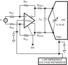 Figure 33. Driving an ADC
The amplifier and ADC muist be located as close together as possible. Both devices require that the filter components be in close proximity to them. The amplifier needs to have minimal parasitic loading on the output traces, and the ADC is sensitive to high-frequency noise that may couple in on its input lines. Some high performance ADCs have an input stage that has a bandwidth of several times its sample rate. The sampling process results in all input signals presented to the input stage mixing down into the Nyquist range (DC to Fs/2). See AN-236 (SNAA079) for more details on the subsampling process and the requirements this imposes on the filtering necessary in your system.
8.1.4 Capacitive Drive
As noted in the Driving Analog to Digital Converters section, capacitive loads should be isolated from the amplifier output with small valued resistors. This is particularly the case when the load has a resistive component that is 500 Ω or higher. A typical ADC has capacitive components of around 8 to 18 pF, and the resistive component could be 1000 Ω or higher. If driving a transmission line, such as a twisted pair, using matching resistors will be sufficient to isolate any subsequent capacitance.
8.2 Typical Application
Figure 34 shows a typical application where an LMP8350 is used to produce a differential signal from a single-ended source.
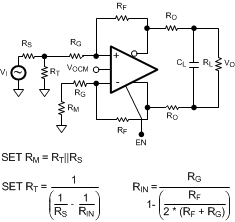 Figure 34. Single-Ended in Differential Out
8.2.1 Design Requirements
Compared to a differential input, using a single-ended input will reduce gain by 1/2, so that the closed-loop gain will be calculated by Equation 4:
In single-ended input operation the output common-mode voltage is set by the VOCM pin. Also, In this mode the common-mode feedback circuit must recreate the signal that is not present on the unused differential input pin. The common-mode feedback circuit is responsible for ensuring balanced output with a single-ended input.
Balance error is defined as the amount of input signal that couples into the output common mode. It is measured as the undesired output common-mode swing divided by the signal on the input. Balance error can be caused by either a channel to channel gain error, or phase error. Either condition will produce a common-mode shift. The overall bandwidth is limited due to the VOCM buffer bandwidth limitations in this configuration.
Supply and VOCM pin bypassing are also critical in this mode of operation.
8.2.2 Detailed Design Procedure
For a single-ended input differential output configuration Figure 34, component value selection is dictated by the gain and input resistance desired. Figure 35 shows the OUT+ and OUT– relative to the single ended voltage signal input +. Depending on the feedback resistor values, the amplitude gain of the OUT+ and OUT– will vary.
8.2.3 Application Curve
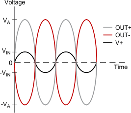 Figure 35. Single-Ended In Differential Out Amplitude vs Time Waveform