SNOSB80C February 2011 – October 2015 LMP8350
PRODUCTION DATA.
7 Detailed Description
7.1 Overview
The LMP8350 is a fully-differential voltage feedback amplifier designed to drive precision differential ADC converters. The LMP8350, though fully integrated for ultimate balance and distortion performance, functionally provides three channels. Two of these channels are the V+ and V− signal path channels, which function similarly to inverting mode operational amplifiers and are the primary signal paths.
The third channel is the common-mode (VOCM) feedback circuit. This is the circuit that sets the output common mode as well as driving the V+ and V− outputs to be equal magnitude and opposite phase, even when only one of the two input channels is driven. The common-mode feedback circuit allows for single-ended to differential operation. The output common-mode voltage is set by applying the appropriate voltage to the VOCM pin.
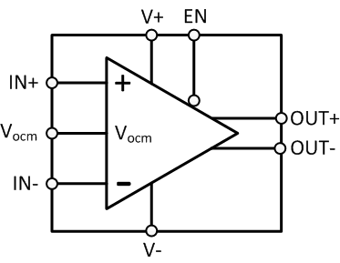
7.2 Functional Block Diagram

7.3 Feature Description
7.3.1 Full Bandwidth Limitations
Although the LMP8350 has a unity gain bandwidth of over 200 MHz, it is primarily intended for lower sample rate, high-precision ADCs with baseband analog input signal bandwidths in the DC to <1 MHz range (not to be confused with sampling rate). The high open-loop bandwidth of the LMP8350 is used to provide ultra low distortion and fast settling times. Maximum power bandwidth is limited by the internal output common-mode feedback path, which is limited to 1 MHz to 5 MHz. Operation with input signals above 1 MHz with near full output swings can cause random shifts in the output common mode and possible AC instabilities. For this reason, the LMP8350 is not intended to be used wide bandwidth (> 1 MHz) signal paths. Single-ended inputs rely on the common-mode signal path and will have a bandwidth limited to that of the internal common-mode buffer.
7.3.2 ESD Protection
The LMP8350 is protected against electrostatic discharge (ESD) on all pins. The LMP8350 will survive 2000-V human body model and 200-V machine model events. Under normal operation, the ESD diodes have no effect on circuit performance. There are occasions, however, when the ESD diodes will be evident. If the LMP8350 is driven by a large signal while the device is powered down the ESD diodes will conduct. The current that flows through the ESD diodes will either exit the chip through the supply pins or will flow through the device, hence it is possible to power up a chip with a large signal applied to the input pins. Using the shutdown mode is one way to conserve power and still prevent unexpected operation.
7.4 Device Functional Modes
7.4.1 Enable Pin and Power Mode Selection
The LMP8350 is equipped with a four-level enable (EN) pin to select one of three power modes or shutdown. These modes are selected by applying the appropriate voltage to the EN pin.
Each power level has a corresponding performance level. The high power mode will have the best overall BW and distortion performance, but at the cost of higher supply current and some DC accuracy. The low power mode has the lowest supply current, but with a noticeable loss of AC performance and output drive capabilities. The mid-power mode provides the best balance of AC and precision DC specifications. In disable mode, the amplifier is shutdown and the output stage goes into a high impedance state. Table 1 summarizes these performance trade-offs.
Table 1. Performance vs. Power Mode Summary
| MODE | VS | –3dB BW (MHz) |
HD2 (dBc) |
NOISE (nV/Hz) |
SR (V/µS) |
TYP VOS (mV) |
|---|---|---|---|---|---|---|
| High | 10 | 118 | –124.7 | 4.6 | 507 | 0.6 |
| 6.6 | 116 | –124.7 | 4.5 | 488 | 0.3 | |
| 5 | 114 | –125.5 | 4.5 | 476 | 0.2 | |
| Med | 10 | 87 | –122.8 | 4.8 | 393 | 0.08 |
| 6.6 | 85 | –122.8 | 4.8 | 376 | 0.1 | |
| 5 | 84 | –122.6 | 4.8 | 366 | 0.1 | |
| Low | 10 | 31 | –117.2 | 8 | 178 | 0.1 |
| 6.6 | 29 | –117.2 | 8 | 166 | 0.1 | |
| 5 | 28 | –117 | 8 | 160 | 0.1 |
To set the mode, internally the voltage at the EN pin is compared against the total supply voltage (VS) and sets the current consumption as shown in the table below. The EN pin voltage is referenced to the V- pin.
Table 2. Enable Pin Mode Selection
| VEN
(VS = V+ - V-) |
POWER MODE |
VEN AT 10 V | VEN AT 6.6 V | VEN AT 5 V | IS
mA |
|---|---|---|---|---|---|
| 7/8 × VS | High | 8.75 | 5.775 | 4.375 | 13 to 15 |
| 5/8 × VS | Med | 6.25 | 4.125 | 3.125 | 7 to 9 |
| 3/8 × VS | Low | 3.75 | 2.475 | 1.875 | 2 to 3 |
| 1/8 × VS | Disable | 1.25 | 0.825 | 0.625 | < 1 |
The enable pin should not be allowed to float. If the enable pin is not used it can be tied to V+ to select the high power mode or set with two resistors.
Each power setting has a ±400-mV tolerance at each level, though TI recommends to keep the set voltage within the center of the range as performance may vary near the transition zones.
During shutdown, both outputs are in a high impedance state, so the feedback and gain set resistors will then set the input and output impedance of the circuit. For this reason input to output isolation will be poor in the disabled state.
The voltage at the EN pin can be generated with a resistive voltage divider or a buffer connected to a voltage source or a DAC. Figure 34 shows how to generate EN voltage with a resistive voltage divider.
Values of RA and RB can be calculated to achieve the voltages in Table 2, however their sum should be below
50 kΩ to keep the voltage at the enable pin stable. Recommended values for RA and RB are given in Table 3.
Table 3. Recommended RA and RB for Mode Selection
| MODE | 10 V | 6.6 V | 5 V | VEN |
|---|---|---|---|---|
| High Power | RA = 0 RB = inf |
RA = 0 RB = inf |
RA = 0 RB = inf |
> 7/8 VS |
| Mid Power | RA = 18 K RB = 30 K |
RA = 18 K RB = 30 K |
RA = 18 K RB = 30 K |
5/8 VS |
| Low Power | RA = 33 K RB = 18 K |
RA = 33 K RB = 18 K |
RA = 33 K RB = 18 K |
3/8 VS |
| Shutdown | RA = Inf RB = 0 |
RA = Inf RB = 0 |
RA = Inf RB = 0 |
< 1/8 VS |
7.4.2 VOCM Pin and Output Common-Mode Setting
Output common-mode voltage is set by the VOCM pin. Both outputs will be offset in the same direction (phase) by an amount equal to the applied VOCM voltage.
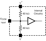
The VOCM pin, if left unconnected, will self-bias to mid-supply. Two internal 60-kΩ resistors set this midpoint. These resistors are shown in Figure 28.
 Figure 28. VOCM Internal Bias Circuit
The equivalent resistance looking into the VOCM pin will look like 30 kΩ to mid-supply, plus about ±700 nA for internal base currents (which scales with power mode and supply current). If left floating, the VOCM input should be bypassed to ground with a 0.1-µF ceramic capacitor.
If a different output common-mode voltage is desired, the VOCM pin should be driven by a clean, low impedance source to override the internal divider resistors. The VOCM pin should be bypassed to ground with a 0.1-µF ceramic capacitor. It should be noted that any signal or noise-coupling into the VOCM will be passed as common-mode noise and may result in the loss of dynamic range, degraded CMRR, degraded balance and higher distortion. The VOCM pin is primarily intended as a DC bias path and is not intended for use as a signal path.
For applications that can tolerate slight shifts in the VOCMvoltage over temperature, it is also possible to use a single resistor to program the VOCM voltage by paralleling one of the internal resistors to change the ratio.