SNOSB80C February   2011  – October 2015 LMP8350

PRODUCTION DATA.  

  1. Features
  2. Applications
  3. Description
  4. Revision History
  5. Pin Configuration and Functions
  6. Specifications
    1. 6.1 Absolute Maximum Ratings
    2. 6.2 ESD Ratings
    3. 6.3 Recommended Operating Conditions
    4. 6.4 Thermal Information
    5. 6.5 10-V Electrical Characteristics
    6. 6.6 6.6-V Electrical Characteristics
    7. 6.7 5-V Electrical Characteristics
    8. 6.8 Typical Characteristics
  7. Detailed Description
    1. 7.1 Overview
    2. 7.2 Functional Block Diagram
    3. 7.3 Feature Description
      1. 7.3.1 Full Bandwidth Limitations
      2. 7.3.2 ESD Protection
    4. 7.4 Device Functional Modes
      1. 7.4.1 Enable Pin and Power Mode Selection
      2. 7.4.2 VOCM Pin and Output Common-Mode Setting
  8. Application and Implementation
    1. 8.1 Application Information
      1. 8.1.1 Fully-Differential Operation
      2. 8.1.2 Single Supply Operation
      3. 8.1.3 Driving Analog to Digital Converters
      4. 8.1.4 Capacitive Drive
    2. 8.2 Typical Application
      1. 8.2.1 Design Requirements
      2. 8.2.2 Detailed Design Procedure
      3. 8.2.3 Application Curve
  9. Power Supply Recommendations
    1. 9.1 Power Supply and VOCM Bypassing
  10. 10Layout
    1. 10.1 Layout Guidelines
    2. 10.2 Layout Example
    3. 10.3 Power Dissipation
    4. 10.4 Evaluation Board
  11. 11Device and Documentation Support
    1. 11.1 Documentation Support
      1. 11.1.1 Related Documentation
    2. 11.2 Community Resources
    3. 11.3 Trademarks
    4. 11.4 Electrostatic Discharge Caution
    5. 11.5 Glossary
  12. 12Mechanical, Packaging, and Orderable Information

パッケージ・オプション

メカニカル・データ(パッケージ|ピン)
サーマルパッド・メカニカル・データ
発注情報

5 Pin Configuration and Functions

D Package
8-Pin SOIC
Top View
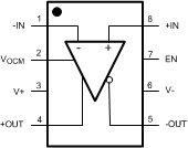
LMP8350 30140502.gif

Pin Functions

PIN I/O DESCRIPTION
NO. NAME
1 –IN I Inverting Input
2 VOCM I Output common-mode voltage set input. Sets output common mode voltage equal to the applied VOCM pin voltage.
3 V+ I Positive power supply voltage
4 +OUT O Noninverting output
5 –OUT O Inverting output
6 V– I Negative power supply voltage
7 EN I Enable and power select input. Applied voltage sets power level or shutdown mode.
8 +IN I Noninverting Input