SNOSB80C February   2011  – October 2015 LMP8350

PRODUCTION DATA.  

  1. Features
  2. Applications
  3. Description
  4. Revision History
  5. Pin Configuration and Functions
  6. Specifications
    1. 6.1 Absolute Maximum Ratings
    2. 6.2 ESD Ratings
    3. 6.3 Recommended Operating Conditions
    4. 6.4 Thermal Information
    5. 6.5 10-V Electrical Characteristics
    6. 6.6 6.6-V Electrical Characteristics
    7. 6.7 5-V Electrical Characteristics
    8. 6.8 Typical Characteristics
  7. Detailed Description
    1. 7.1 Overview
    2. 7.2 Functional Block Diagram
    3. 7.3 Feature Description
      1. 7.3.1 Full Bandwidth Limitations
      2. 7.3.2 ESD Protection
    4. 7.4 Device Functional Modes
      1. 7.4.1 Enable Pin and Power Mode Selection
      2. 7.4.2 VOCM Pin and Output Common-Mode Setting
  8. Application and Implementation
    1. 8.1 Application Information
      1. 8.1.1 Fully-Differential Operation
      2. 8.1.2 Single Supply Operation
      3. 8.1.3 Driving Analog to Digital Converters
      4. 8.1.4 Capacitive Drive
    2. 8.2 Typical Application
      1. 8.2.1 Design Requirements
      2. 8.2.2 Detailed Design Procedure
      3. 8.2.3 Application Curve
  9. Power Supply Recommendations
    1. 9.1 Power Supply and VOCM Bypassing
  10. 10Layout
    1. 10.1 Layout Guidelines
    2. 10.2 Layout Example
    3. 10.3 Power Dissipation
    4. 10.4 Evaluation Board
  11. 11Device and Documentation Support
    1. 11.1 Documentation Support
      1. 11.1.1 Related Documentation
    2. 11.2 Community Resources
    3. 11.3 Trademarks
    4. 11.4 Electrostatic Discharge Caution
    5. 11.5 Glossary
  12. 12Mechanical, Packaging, and Orderable Information

パッケージ・オプション

メカニカル・データ(パッケージ|ピン)
サーマルパッド・メカニカル・データ
発注情報

9 Power Supply Recommendations

9.1 Power Supply and VOCM Bypassing

The LMP8350 requires supply bypassing capacitors as shown in Figure 36 and Figure 37 for fastest settling time and overall stability.
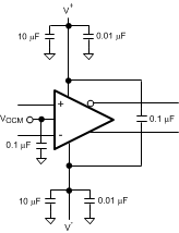
LMP8350 30140553.gif Figure 36. Split-Supply Bypassing Capacitors

The 0.01-µF and 0.1-µF capacitors should be leadless surface mount (SMT) ceramic capacitors and should be no more than 3 mm from the supply pins. The SMT capacitors should be connected directly to a ground plane. Thin traces or small vias will reduce the effectiveness of bypass capacitors.
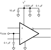
LMP8350 30140554.gif Figure 37. Single-Supply Bypassing Capacitors

Also shown in Figure 36 and Figure 37 is a capacitor from the VOCM pin to ground. The VOCM pin sets the output common-mode voltage. Any noise on this input is transferred directly to the output. The VOCM pin should be bypassed even if the pin in not used. There is an internal resistive divider on chip to set the output common-mode voltage to the midpoint of the supply pins. The impedance looking into this pin is approximately 30 kΩ. If a different output common-mode voltage is desired drive this pin with a clean, accurate voltage reference.