SNOSC63B February   2012  – December 2014 LMP8646

PRODUCTION DATA.  

  1. Features
  2. Applications
  3. Description
    1.     Device Images
      1.      Typical Application
  4. Revision History
  5. Pin Configuration and Functions
    1.     Pin Functions
  6. Specifications
    1. 6.1 Absolute Maximum Ratings
    2. 6.2 ESD Ratings
    3. 6.3 Recommended Operating Conditions
    4. 6.4 Thermal Information
    5. 6.5 Electrical Characteristics: 2.7 V
    6. 6.6 Electrical Characteristics: 5 V
    7. 6.7 Electrical Characteristics: 12 V
    8. 6.8 Typical Characteristics
  7. Detailed Description
    1. 7.1 Overview
    2. 7.2 Functional Block Diagram
    3. 7.3 Feature Description
      1. 7.3.1 Theory of Operation
        1. 7.3.1.1 Maximum Output Voltage, VOUT_MAX
          1. 7.3.1.1.1 Case 1: −2 V < VCM < 1.8 V, and VS > 2.7 V
          2. 7.3.1.1.2 Case 2: 1.8 V < VCM < VS, and VS > 3.3 V
          3. 7.3.1.1.3 Case 3: VCM > VS, and VS > 2.7 V
    4. 7.4 Device Functional Modes
      1. 7.4.1 Output Accuracy
      2. 7.4.2 Selection of the Sense Resistor, RSENSE
        1. 7.4.2.1 RSENSE Consideration for System Error
  8. Application and Implementation
    1. 8.1 Application Information
    2. 8.2 Typical Applications
      1. 8.2.1 Application #1: Current Limiter With a Capacitive Load
        1. 8.2.1.1 Design Requirements
        2. 8.2.1.2 Detailed Design Procedure
        3. 8.2.1.3 Application Curve
      2. 8.2.2 Application #2: Current Limiter With a Resistive Load
        1. 8.2.2.1 Design Requirements
        2. 8.2.2.2 Detailed Design Procedure
        3. 8.2.2.3 Application Curve
      3. 8.2.3 Application #3: Current Limiter With a Low-Dropout Regulator and Resistive Load
        1. 8.2.3.1 Design Requirements
        2. 8.2.3.2 Detailed Design Procedure
        3. 8.2.3.3 Application Curve
  9. Power Supply Recommendations
  10. 10Layout
    1. 10.1 Layout Guidelines
    2. 10.2 Layout Example
  11. 11Device and Documentation Support
    1. 11.1 Trademarks
    2. 11.2 Electrostatic Discharge Caution
    3. 11.3 Glossary
  12. 12Mechanical, Packaging, and Orderable Information

パッケージ・オプション

メカニカル・データ(パッケージ|ピン)
サーマルパッド・メカニカル・データ
発注情報

Theory of Operation

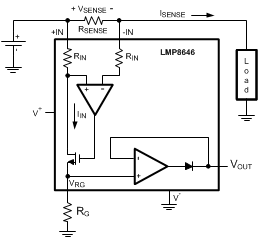
As seen from Figure 26, the sense current flowing through RSENSE develops a voltage drop equal to VSENSE. The high impedance inputs of the amplifier does not conduct this current and the high open-loop gain of the sense amplifier forces its noninverting input to the same voltage as the inverting input. In this way the voltage drop across RIN matches VSENSE. The current IIN flowing through RIN has the following equation:

Equation 1. IIN = VSENSE/ RIN = RSENSE*ISENSE/RIN

where

  • RIN = 1/Gm = 1/(200 µA/V) = 5 kOhm

IIN flows entirely across the external gain resistor RG to develop a voltage drop equal to:

Equation 2. VRG = IIN*RG = (VSENSE/RIN) *RG = [(RSENSE*ISENSE) / RIN]*RG


This voltage is buffered and showed at the output with a very low impedance allowing a very easy interface of the LMP8646 with the feedback of many voltage regulators. This output voltage has the following equation:

Equation 3. VOUT = VRG = [(RSENSE*ISENSE) / RIN]*RG
Equation 4. VOUT = VSENSE* RG/RIN
Equation 5. VOUT = VSENSE* RG/(5 kOhm)
Equation 6. VOUT = VSENSE* Gain

where

  • Gain = RG/RIN
LMP8646 30123503.gifFigure 26. Current Monitor