SNOSC63B February 2012 – December 2014 LMP8646
PRODUCTION DATA.
- 1 Features
- 2 Applications
- 3 Description
- 4 Revision History
- 5 Pin Configuration and Functions
- 6 Specifications
- 7 Detailed Description
- 8 Application and Implementation
- 9 Power Supply Recommendations
- 10Layout
- 11Device and Documentation Support
- 12Mechanical, Packaging, and Orderable Information
6.8 Typical Characteristics
Unless otherwise specified: TA = 25°C, VS= V+ - V-, VSENSE= +IN - (-IN), RL = 10 kΩ.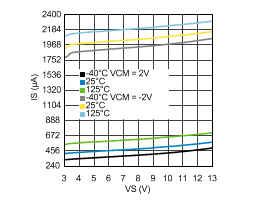 Figure 1. Supply Curent vs. Supply Voltage for VCM = 2 V
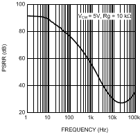 Figure 3. AC PSRR vs. Frequency
 Figure 5. CMRR vs. High VCM
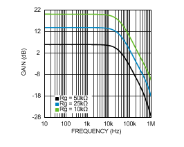 Figure 7. Gain vs. Frequency (BW = 35 kHz)
 Figure 9. Gain Accuracy vs. VCM
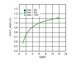 Figure 11. VOUT_MAX vs. Gain at Vs = 2.7 V
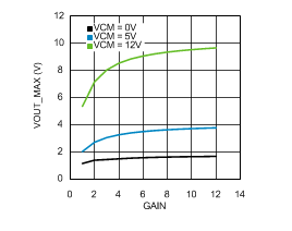 Figure 13. VOUT_MAX vs. Gain at Vs = 12 V
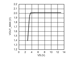 Figure 15. VOUT_MAX vs. VS at VCM = 2.1 V
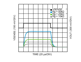 Figure 17. Large Step Response at BW = 35 kHz
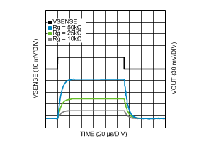 Figure 19. Small Step Response at BW = 35 kHz
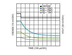 Figure 21. Settling Time (Fall) at 1 kHz
 Figure 23. Settling Time (Fall) at 35 kHz
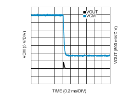 Figure 25. Common-Mode Step Response (Fall) at 35 kHz
 Figure 2. Supply Current vs. VCM
 Figure 4. AC CMRR vs. Frequency
 Figure 6. Gain vs. Frequency (BW = 1kHz)
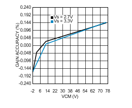 Figure 8. Gain Accuracy vs. VCM
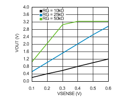 Figure 10. VOUT vs. VSENSE
 Figure 12. VOUT_MAX vs. Gain at Vs = 5.0 V
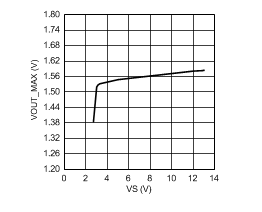 Figure 14. VOUT_MAX vs. VS at VCM = –2 V
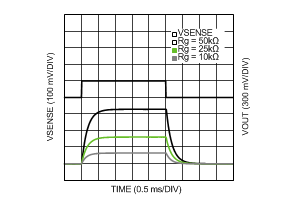 Figure 16. Large Step Response at BW = 1kHz
 Figure 18. Small Step Response at BW = 1 kHz
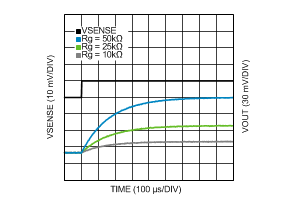 Figure 20. Settling Time (Rise) at 1 kHz
 Figure 22. Settling Time (Rise) at 35 kHz
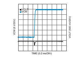 Figure 24. Common-Mode Step Response (Rise) at 35 kHz