JAJSHJ4C October 2011 – June 2019 LMR10510
PRODUCTION DATA.
- 1 特長
- 2 アプリケーション
- 3 概要
- 4 改訂履歴
- 5 概要(続き)
- 6 Pin Configuration and Functions
- 7 Specifications
- 8 Detailed Description
- 9 Application and Implementation
- 10Layout
- 11デバイスおよびドキュメントのサポート
- 12メカニカル、パッケージ、および注文情報
パッケージ・オプション
メカニカル・データ(パッケージ|ピン)
サーマルパッド・メカニカル・データ
発注情報
9.2.1.2 Inductor Selection
The duty cycle (D) can be approximated quickly using the ratio of output voltage (VO) to input voltage (VIN):

The catch diode (D1) forward voltage drop and the voltage drop across the internal PMOS must be included to calculate a more accurate duty cycle. Calculate D by using the following formula:

VSW can be approximated by:
The diode forward drop (VD) can range from 0.3 V to 0.7 V depending on the quality of the diode. The lower the VD, the higher the operating efficiency of the converter. The inductor value determines the output ripple current. Lower inductor values decrease the size of the inductor, but increase the output ripple current. An increase in the inductor value will decrease the output ripple current.
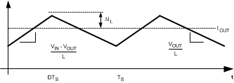
One must ensure that the minimum current limit (1.2 A) is not exceeded, so the peak current in the inductor must be calculated. The peak current (ILPK) in the inductor is calculated by:
 Figure 16. Inductor Current
In general,
If ΔiL = 20% of 1 A, the peak current in the inductor will be 1.2 A. The minimum specified current limit over all operating conditions is 1.2 A. One can either reduce ΔiL, or make the engineering judgment that zero margin will be safe enough. The typical current limit is 1.75 A.
The LMR10510 operates at frequencies allowing the use of ceramic output capacitors without compromising transient response. Ceramic capacitors allow higher inductor ripple without significantly increasing output ripple. See the Output Capacitor section for more details on calculating output voltage ripple. Now that the ripple current is determined, the inductance is calculated by:

where
When selecting an inductor, make sure that it is capable of supporting the peak output current without saturating. Inductor saturation will result in a sudden reduction in inductance and prevent the regulator from operating correctly. Because of the speed of the internal current limit, the peak current of the inductor need only be specified for the required maximum output current. For example, if the designed maximum output current is 1 A and the peak current is 1.25 A, then the inductor should be specified with a saturation current limit of > 1.25A. There is no need to specify the saturation or peak current of the inductor at the 1.75 A typical switch current limit. The difference in inductor size is a factor of 5. Because of the operating frequency of the LMR10510, ferrite based inductors are preferred to minimize core losses. This presents little restriction since the variety of ferrite-based inductors is huge. Lastly, inductors with lower series resistance (RDCR) will provide better operating efficiency. For recommended inductors see examples in Other System Examples.
