LMR14006 SIMPLE SWITCHER 40 V 600 mA Buck Regulator With High Efficiency Sleep Mode
1 Features
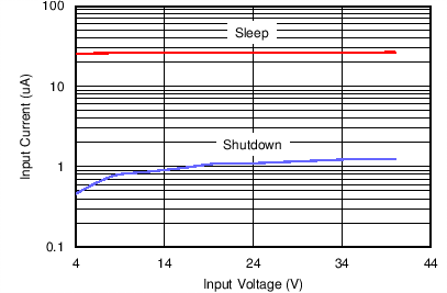
- Ultra Low 28 µA Standby Current in Sleep Mode
- Input Voltage Range 4 V to 40 V
- 1 µA Shutdown Current
- High Duty Cycle Operation Supported
- Output Current up to 600 mA
- 1.1 MHz and 2.1 MHz Switching Frequency
- Internal Compensation
- High Voltage Enable Input
- Internal Soft Start
- Over Current Protection
- Over Temperature Protection
- Small Overall Solution Size (TSOT-6L Package)
2 Applications
- Industrial Distributed Power Systems
- Automotive
- Battery Powered Equipment
- Portable Handheld Instruments
- Portable Media Players
3 Description
The LMR14006 is a PWM DC/DC buck (step-down) regulator. With a wide input range of 4 V-40 V, it is suitable for a wide range of application from industrial to automotive for power conditioning from an unregulated source. The regulator’s standby current is 28 µA in sleep mode, which is suitable for battery operating systems. An ultra low 1 µA current can further prolong battery life in shutdown mode. Operating frequency is fixed at 1.1 MHz (X version) and 2.1 MHz (Y version) allowing the use of small external components while still being able to have low output ripple voltage. Soft-start and compensation circuits are implemented internally, and these allow the device to be used with minimized external components. The LMR14006 is optimized for up to 600 mA load current which has a 0.765 V typical feedback voltage. The device has built-in protection features such as pulse by pulse current limit, thermal sensing and shutdown due to excessive power dissipation. The LMR14006 is available in a low profile TSOT-6L package.
Device Information(1)
| PART NUMBER | PACKAGE | BODY SIZE (NOM) |
|---|---|---|
| LMR14006 | TSOT-6L | 2.9mm × 1.6 mm |
- For all available packages, see the orderable addendum at the end of the datasheet.
 Figure 1. Typical Application Schematic
4 Revision History
Changes from * Revision (November 2013) to A Revision
- Deleted the other part number LMR14003 from the rest of the document Go
- Added Device Information and Handling Rating tables, Feature Description, Application and Implementation, , Layout, Device and Documentation Support, and Mechanical, Packaging, and Orderable Information sections; moved some curves to Application Curves sectionGo
- Changed from 2kV to 1kVGo
Changes from A Revision (September 2014) to B Revision
5 Pin Configuration and Functions

Pin Functions
| PIN | I/O | DESCRIPTION | |
|---|---|---|---|
| NAME | NUMBER | ||
| CB | 1 | I | SW FET Gate Bias voltage. Connect Cboot cap between CB and SW |
| GND | 2 | G | Ground Connection |
| FB | 3 | I | Feedback Pin. Set feedback voltage divider ratio with VOUT = VFB (1+(R1/R2)) |
| /SHDN | 4 | I | Enable and disable input pin(high voltage tolerant). Internal pull-up current source. Pull below 1.2V to disable. Float to enable. Adjust the input undervoltage lockout with two resistors. |
| VIN | 5 | I | Power input voltage pin. Input for internal supply and drain node input for internal high-side MOSFET |
| SW | 6 | O | Switch node. Connect to inductor, diode, and Cboot cap |
6 Specifications
6.1 Absolute Maximum Ratings
over operating free-air temperature range (unless otherwise noted) (1)6.2 Handling Ratings
| MIN | MAX | UNIT | |||
|---|---|---|---|---|---|
| Tstg | Storage temperature range | -55 | 165 | °C | |
| V(ESD) | Electrostatic discharge | Human body model (HBM), per ANSI/ESDA/JEDEC JS-001, all pins except CB pin(1) | 1000 | V | |
| Charged device model (CDM), per JEDEC specification JESD22-C101, all pins(2) | 500 | ||||
6.3 Recommended Operating Conditions (1)
Over operating free-air temperature range (unless otherwise noted)| PARAMETER | MIN | MAX | UNIT | |
|---|---|---|---|---|
| Buck Regulator | VIN | 4 | 40 | V |
| CB | 4 | 46 | V | |
| CB to SW | -0.3 | 6 | V | |
| SW | -1 | 40 | ||
| FB | 0 | 5.5 | V | |
| Control | SHDN | 0 | 40 | V |
| Temperature | Operating junction temperature range, TJ | -40 | 125 | °C |
6.4 Thermal Information
| THERMAL METRIC (1) | TSOT (6 PINS) |
UNIT | |
|---|---|---|---|
| RθJA | Junction-to-ambient thermal resistance | 102 | °C/W |
| RθJCtop | Junction-to-case (top) thermal resistance | 36.9 | |
| RθJB | Junction-to board characterization parameter | 28.4 |
6.5 Electrical Characteristics
VIN = /SHDN = 12V, TA = 25°C, unless otherwise specified.| SYMBOL | PARAMETER | CONDITIONS | MIN | TYP | MAX | UNIT | |
|---|---|---|---|---|---|---|---|
| VIN (Input Power Supply) | |||||||
| VIN | Operating input voltage | 4 | 40 | V | |||
| ISHDN | Shutdown supply current | VEN = 0V | 1 | 3 | µA | ||
| IQ | Operating quiescent current (non- switching) | no load, VIN = 12V | 28 | µA | |||
| UVLO | Undervoltage lockout thresholds | Rising threshold | 4 | V | |||
| Falling threshold | 3 | ||||||
| SHDN | |||||||
| VSHDN_Thre | Rising SHDN Threshold Voltage | 1.05 | 1.25 | 1.38 | V | ||
| ISHDN_PIN | Input current | SHDN = 2.3V | –4.2 | µA | |||
| SHDN = 0.9V | –1 | ||||||
| ISHDN_HYS | Hysteresis current | –3 | µA | ||||
| HIGH-SIDE MOSFET | |||||||
| RDS_ON | On-resistance | VIN = 12V, CB to SW = 5.8V | 600 | mΩ | |||
| VOLTAGE REFERENCE (FB PIN) | |||||||
| VFB | Feedback voltage | 0.747 | 0.765 | 0.782 | V | ||
| CURRENT LIMIT | |||||||
| ILIMIT | Current limit | VIN = 12V, TJ = 25°C | 1200 | mA | |||
| THERMAL PERFORMANCE | |||||||
| TSHDN | Thermal shutdown threshold | 170 | ºC | ||||
| THYS | Hysteresis | 10 | ºC | ||||
6.6 Switching Characteristics
Over operating free-air temperature range (unless otherwise noted)| PARAMETER | TEST CONDITIONS | MIN | TYP | MAX | UNIT | |
|---|---|---|---|---|---|---|
| SW (SW PIN) | ||||||
| fSW | Switching frequency | LMR14006X | 935 | 1100 | 1285 | kHz |
| LMR14006Y | 1785 | 2100 | 2415 | |||
| TON_MIN | Minimum turn-on time | fSW = 2.1 MHz | 95 | ns | ||
| DMAX | Maximum duty cycle | LMR14006X | 96% | |||
| LMR14006Y | 97% | |||||
6.7 Typical Characteristics
VIN = 12V, TA = 25°C, unless otherwise specified.
| fSW = 2.1 MHz | VOUT = 12 V | |
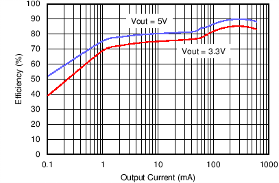
| fSW = 2.1 MHz | ||

| VOUT = 5 V | ||


| fSW = 2.1 MHz | VOUT = 5 V | |

| IOUT = 200 mA | VOUT = 5 V | |
7 Detailed Description
7.1 Overview
The LMR14006 device is a 40 V, 600 mA, step-down (buck) regulator. The buck regulator has a very low quiescent current during light load to prolong the battery life.
For LMR14006, to improve performance during line and load transients it implements a constant frequency, current mode control which requires less output capacitance and simplifies frequency compensation design. Two switching frequency options, 1.1 MHz and 2.1 MHz, are available, thus smaller inductor and capacitor can be used. The LMR14006 reduces the external component count by integrating the boot recharge diode. The bias voltage for the integrated high side MOSFET is supplied by a capacitor on the CB to SW pin. The boot capacitor voltage is monitored by an UVLO circuit and will turn the high side MOSFET off when the boot voltage falls below a preset threshold. The LMR14006 can operate at high duty cycles because of the boot UVLO and refresh wimp FET. The output voltage can be stepped down to as low as the 0.8 V reference. Internal soft start is featured to minimize inrush currents.
7.2 Functional Block Diagram

7.3 Feature Description
7.3.1 Continuous Conduction Mode
The LMR14006 steps the input voltage down to a lower output voltage. In continuous conduction mode (when the inductor current never reaches zero at steady state), the buck regulator operates in two cycles. The power switch is connected between VIN and SW. In the first cycle of operation the transistor is closed and the diode is reverse biased. Energy is collected in the inductor and the load current is supplied by Cout and the rising current through the inductor. During the second cycle the transistor is open and the diode is forward biased due to the fact that the inductor current cannot instantaneously change direction. The energy stored in the inductor is transferred to the load and output capacitor. The ratio of these two cycles determines the output voltage. The output voltage is defined approximately as: D = VOUT/VIN and D' = (1-D) where D is the duty cycle of the switch, D and D' will be required for design calculations.
7.3.2 Fixed Frequency Pwm Control
The LMR14006 has two fixed frequency options, and it implements peak current mode control. The output voltage is compared through external resistors on the VFB pin to an internal voltage reference by an error amplifier which drives the internal COMP node. An internal oscillator initiates the turn on of the high side power switch. The error amplifier output is compared to the high side power switch current. When the power switch current reaches the level set by the internal COMP voltage, the power switch is turned off. The internal COMP node voltage will increase and decrease as the output current increases and decreases. The device implements a current limit by clamping the COMP node voltage to a maximum level.
7.3.3 Sleep Mode
The LMR14006 operates in sleep mode at light load currents to improve efficiency by reducing switching and gate drive losses. The LMR14006 is designed so that if the output voltage is within regulation and the peak switch current at the end of any switching cycle is below the sleep current threshold, IINDUCTOR ≤ 80 mA, the device enters sleep mode. For sleep mode operation, the LMR14006 senses peak current, not average or load current, so the load current where the device enters sleep mode is dependent on the output inductor value. When the load current is low and the output voltage is within regulation, the device enters a sleep mode and draws only 28 µA input quiescent current.
7.3.4 Bootstrap Voltage (CB)
The LMR14006 has an integrated boot regulator, and requires a small ceramic capacitor between the CB and SW pins to provide the gate drive voltage for the high side MOSFET. The CB capacitor is refreshed when the high side MOSFET is off and the low side diode conducts. To improve drop out, the LMR14006 is designed to operate at 100% duty cycle as long as the CB to SW pin voltage is greater than 3 V. When the voltage from CB to SW drops below 3V, the high side MOSFET is turned off using an UVLO circuit which allows the low side diode to conduct and refresh the charge on the CB capacitor. Since the supply current sourced from the CB capacitor is low, the high side MOSFET can remain on for more switching cycles than are required to refresh the capacitor, thus the effective duty cycle of the switching regulator is high. Attention must be taken in maximum duty cycle applications with light load. To ensure SW can be pulled to ground to refresh the CB capacitor, an internal circuit will charge the CB capacitor when the load is light or the device is working in dropout condition.
7.3.5 Output Voltage Setting
The output voltage is set using the feedback pin and a resistor divider connected to the output as shown in Functional Block Diagram. The feedback pin voltage 0.765V, so the ratio of the feedback resistors sets the output voltage according to the following equation: VOUT = 0.765V (1+(R1/R2)) Typically R2 will be given as 100 Ω - 10 kΩ for a starting value. To solve for R1 given R2 and Vout uses R1 = R2 ((VOUT/0.765V)-1).
7.3.6 Enable (/SHDN) and VIN Under Voltage Lockout
LMR14006 /SHDN pin is a high voltage tolerant input with an internal pull up circuit. The device can be enabled even if the /SHDN pin is floating. The regulator can also be turned on using 1.23V or higher logic signals. If the use of a higher voltage is desired due to system or other constraints, a 100 kΩ or larger resistor is recommended between the applied voltage and the /SHDN pin to protect the device. When /SHDN is pulled down to 0V, the chip is turned off and enters the lowest shutdown current mode. In shutdown mode the supply current will be decreased to approximately 1 µA. If the shutdown function is not to be used the /SHDN pin may be tied to VIN. The maximum voltage to the SHDN pin should not exceed 40V. LMR14006 has an internal UVLO circuit to shutdown the output if the input voltage falls below an internally fixed UVLO threshold level. This ensures that the regulator is not latched into an unknown state during low input voltage conditions. The regulator will power up when the input voltage exceeds the voltage level. If there is a requirement for a higher UVLO voltage, the /SHDN can be used to adjust the input voltage UVLO by using external resistors.
7.3.7 Current Limit
The LMR14006 implements current mode control which uses the internal COMP voltage to turn off the high side MOSFET on a cycle-by-cycle basis. Each cycle the switch current and internal COMP voltage are compared, when the peak switch current intersects the COMP voltage, the high side switch is turned off. During overcurrent conditions that pull the output voltage low, the error amplifier will respond by driving the COMP node high, increasing the switch current. The error amplifier output is clamped internally, which functions as a switch current limit.
7.3.8 Overvoltage Transient Protection
The LMR14006 incorporates an overvoltage transient protection (OVTP) circuit to minimize voltage overshoot when recovering from output fault conditions or strong unload transients on power supply designs with low value output capacitance. For example, when the power supply output is overloaded the error amplifier compares the actual output voltage to the internal reference voltage. If the FB pin voltage is lower than the internal reference voltage for a considerable time, the output of the error amplifier will respond by clamping the error amplifier output to a high voltage. Thus, requesting the maximum output current. Once the condition is removed, the regulator output rises and the error amplifier output transitions to the steady state duty cycle. In some applications, the power supply output voltage can respond faster than the error amplifier output can respond, this actuality leads to the possibility of an output overshoot. The OVTP feature minimizes the output overshoot, when using a low value output capacitor, by implementing a circuit to compare the FB pin voltage to OVTP threshold which is 108% of the internal voltage reference. If the FB pin voltage is greater than the OVTP threshold, the high side MOSFET is disabled preventing current from flowing to the output and minimizing output overshoot. When the FB voltage drops lower than the OVTP threshold, the high side MOSFET is allowed to turn on at the next clock cycle.
7.3.9 Thermal Shutdown
The device implements an internal thermal shutdown to protect itself if the junction temperature exceeds 170°C(typ). The thermal shutdown forces the device to stop switching when the junction temperature exceeds the thermal trip threshold. Once the junction temperature decreases below 160°C(typ), the device reinitiates the power up sequence.
8 Applications and Implementation
NOTE
Information in the following applications sections is not part of the TI component specification, and TI does not warrant its accuracy or completeness. TI’s customers are responsible for determining suitability of components for their purposes. Customers should validate and test their design implementation to confirm system functionality.
8.1 Typical Applications
 Figure 9. LMR14006 Design Example with 2.1 MHz Switching Frequency
Below are the recommended typical output voltage inductor/capacitor combinations for optimized total solution size.
| P/N | Vout(V) | R1(kΩ) | R2(kΩ) | L(μH) | Cout(μF) |
|---|---|---|---|---|---|
| LMR14006 Y | 5 | 54.9(1%) | 10(1%) | 3.3 | 22 |
| LMR14006 Y | 12 | 147(1%) | 10(1%) | 3.3 | 10 |
 Figure 10. Application Circuit, 12 V Output
8.1.1 Design Requirements
This example details the design of a high frequency switching regulator using ceramic output capacitors. A few parameters must be known in order to start the design process. These parameters are typically determined at the system level:
Table 1. Design Parameters
| Input Voltage, VIN | 9V to 16V, Typical 12V | |
| Output Voltage, VOUT | 5.0V ± 3% | |
| Maximum Output Current IO_max | 0.6A | |
| Minimum Output Current IO_min | 0.03A | |
| Transient Response 0.03A to 0.6A | 5% | |
| Output Voltage Ripple | 1% | |
| Switching Frequency Fsw | 2.1MHz | |
| Target during Load Transient | Over Voltage Peak Value | 106% of Output Voltage |
| Under Voltage Value | 91% of Output Voltage | |
8.1.2 Detailed Design Procedure
8.1.2.1 Selecting The Switching Frequency
The first step is to decide on a switching frequency for the regulator. Typically, the user will want to choose the highest switching frequency possible since this will produce the smallest solution size. The high switching frequency allows for lower valued inductors and smaller output capacitors compared to a power supply that switches at a lower frequency. The switching frequency that can be selected is limited by the minimum on-time of the internal power switch, the input voltage and the output voltage and the frequency shift limitation. For this example, the output voltage is 5V and the maximum input voltage is 16 V, a switching frequency of 2100 kHz is used.
8.1.2.2 Output Inductor Selection
The most critical parameters for the inductor are the inductance, peak current and the DC resistance. The inductance is related to the peak-to-peak inductor ripple current, the input and the output voltages. Since the ripple current increases with the input voltage, the maximum input voltage is always used to determine the inductance. To calculate the minimum value of the output inductor, use Equation 1. KIND is a coefficient that represents the amount of inductor ripple current relative to the maximum output current. A reasonable value is setting the ripple current to be 30% of the DC output current. For this design example, the minimum inductor value is calculated to be 9.1 µH, and a nearest standard value was chosen: 10 µH. For the output filter inductor, it is important that the RMS current and saturation current ratings not be exceeded. The RMS and peak inductor current can be found from Equation 3 and Equation 4. The inductor ripple current is 0.16 A, and the RMS current is 0.602 A. As the equation set demonstrates, lower ripple currents will reduce the output voltage ripple of the regulator but will require a larger value of inductance. A good starting point for most applications is a 10 μH with 2 A current rating. Using a rating near 2 A will enable the LMR14006 to current limit without saturating the inductor. This is preferable to the LMR14006 going into thermal shutdown mode and the possibility of damaging the inductor if the output is shorted to ground or other long-term overload.


8.1.2.3 Output Capacitor
The selection of COUT is mainly driven by three primary considerations. The output capacitor will determine the modulator pole, the output voltage ripple, and how the regulator responds to a large change in load current. The output capacitance needs to be selected based on the most stringent of these three criteria.
The desired response to a large change in the load current is the first criteria. The regulator usually needs two or more clock cycles for the control loop to see the change in load current and output voltage and adjust the duty cycle to react to the change. The output capacitance must be large enough to supply the difference in current for 2 clock cycles while only allowing a tolerable amount of droop in the output voltage. Equation 5 shows the minimum output capacitance necessary to accomplish this. For this example, the transient load response is specified as a 3% change in VOUT for a load step from 0.03A to 0.6A (full load). For this example, ΔIOUT = 0.6 -0.03 = 0.57 A and ΔVOUT = 0.03 × 5 = 0.15 V. Using these numbers gives a minimum capacitance of 3.6µF. For ceramic capacitors, the ESR is usually small enough to ignore in this calculation. Aluminum electrolytic and tantalum capacitors have higher ESR that should be taken into account.
The stored energy in the inductor will produce an output voltage overshoot when the load current rapidly decreases. The output capacitor must also be sized to absorb energy stored in the inductor when transitioning from a high load current to a lower load current. Equation 6 is used to calculate the minimum capacitance to keep the output voltage overshoot to a desired value. Where L is the value of the inductor, IOH is the output current under heavy load, IOL is the output under light load, Vf is the final peak output voltage, and Vi is the initial capacitor voltage. For this example, the worst case load step will be from 0.6 A to 0.03 A. The output voltage will increase during this load transition and the stated maximum in our specification is 3% of the output voltage. This will make Vo_overshoot = 1.03 × 5 = 5.15 V. Vi is the initial capacitor voltage which is the nominal output voltage of 5V. Using these numbers in Equation 6 yields a minimum capacitance of 2.36 µF.
Equation 7 calculates the minimum output capacitance needed to meet the output voltage ripple specification. Where fsw is the switching frequency, Vo_ripple is the maximum allowable output voltage ripple, and IL_ripple is the inductor ripple current. Equation 7 yields 0.21µF.
Equation 8 calculates the maximum ESR an output capacitor can have to meet the output voltage ripple specification. Equation 8 indicates the ESR should be less than 277mΩ.
Additional capacitance de-ratings for aging, temperature and dc bias should be factored in which will increase this minimum value. For this example, 10µF ceramic capacitors will be used. Capacitors in the range of 4.7µF-100µF are a good starting point with an ESR of 0.1Ω or less.


8.1.2.4 Schottky Diode
The breakdown voltage rating of the diode is preferred to be 25% higher than the maximum input voltage. The current rating for the diode should be equal to the maximum output current for best reliability in most applications. In cases where the input voltage is much greater than the output voltage the average diode current is lower. In this case it is possible to use a diode with a lower average current rating, approximately (1-D) × IOUT however the peak current rating should be higher than the maximum load current. A 0.5A to 1A rated diode is a good starting point.
8.1.2.5 Input Capacitor
A low ESR ceramic capacitor is needed between the VIN pin and ground pin. This capacitor prevents large voltage transients from appearing at the input. Use a 1µF-10µF value with X5R or X7R dielectric. Depending on construction, a ceramic capacitor’s value can decrease up to 50% of its nominal value when rated voltage is applied. Consult with the capacitor manufactures data sheet for information on capacitor derating over voltage and temperature. The capacitor must also have a ripple current rating greater than the maximum input current ripple of the LMR14006. The input ripple current can be calculated using below Equation 9.
For this example design, one 2.2µF, 50V capacitor is selected. The input capacitance value determines the input ripple voltage of the regulator. The input voltage ripple can be calculated using Equation 10. Using the design example values, IOUTmax = 0.6A, CIN = 2.2µF, ƒSW = 2100kHz, yields an input voltage ripple of 32.5mV and a rms input ripple current of 0.3A.


8.1.2.6 Bootstrap Capacitor Selection
A 0.1μF ceramic capacitor or larger is recommended for the bootstrap capacitor (CBOOT). For applications where the input voltage is close to output voltage a larger capacitor is recommended, generally 0.1 µF to 1 µF to ensure plenty of gate drive for the internal switches and a consistently low RDSON. A ceramic capacitor with an X7R or X5R grade dielectric with a voltage rating of 10V or higher is recommended because of the stable characteristics over temperature and voltage.
8.1.3 Application Performance Curves

| Vout = 5 V | 600 mA Load | |

| Vin = 18 V | 300 mA Load | |


| Vin = 18V | 300 mA Load | |

