SNVSAG4B November 2015 – December 2024 LMR14020-Q1
PRODUCTION DATA
- 1
- 1 Features
- 2 Applications
- 3 Description
- 4 Pin Configuration and Functions
- 5 Specifications
-
6 Detailed Description
- 6.1 Overview
- 6.2 Functional Block Diagram
- 6.3
Feature Description
- 6.3.1 Fixed Frequency Peak Current Mode Control
- 6.3.2 Slope Compensation
- 6.3.3 Sleep Mode
- 6.3.4 Low Dropout Operation and Bootstrap Voltage (BOOT)
- 6.3.5 Adjustable Output Voltage
- 6.3.6 Enable and Adjustable Undervoltage Lockout
- 6.3.7 External Soft-start
- 6.3.8 Switching Frequency and Synchronization (RT/SYNC)
- 6.3.9 Power Good (PGOOD)
- 6.3.10 Overcurrent and Short-Circuit Protection
- 6.3.11 Overvoltage Protection
- 6.3.12 Thermal Shutdown
- 6.4 Device Functional Modes
- 7 Application and Implementation
- 8 Device and Documentation Support
- 9 Revision History
- 10Mechanical, Packaging, and Orderable Information
パッケージ・オプション
メカニカル・データ(パッケージ|ピン)
サーマルパッド・メカニカル・データ
- DDA|8
発注情報
3 Description
The LMR14020-Q1 is a 40V, 2A step-down regulator with an integrated high-side MOSFET. With a wide input range from 4V to 40V, the device is designed for various applications from industrial to automotive for power conditioning from unregulated sources. An extended family is available in 3.5A and 5A options in pin-to-pin compatible packages, including LMR14030-Q1 and LMR14050-Q1. The regulator quiescent current is 40µA in sleep mode, which is designed for battery powered systems. An ultra-low 1μA current in shutdown mode can further prolong battery life. A wide adjustable switching frequency range allows either efficiency or external component size to be optimized. Internal loop compensation means that the user is free from the tedious task of loop compensation design. This internal loop compensation also minimizes the external components of the device. A precision enable input allows simplification of regulator control and system power sequencing. The device also has built-in protection features such as cycle-by-cycle current limit, thermal sensing and shutdown due to excessive power dissipation, and output overvoltage protection.
The LMR14020-Q1 is available in an 8-pin, HSOIC or 10-pin, WSON package with exposed pad for low thermal resistance.
| PART NUMBER | PACKAGE(1) | PACKAGE SIZE(2) |
|---|---|---|
| LMR14020SQDDARQ1 | DDA (HSOIC, 8) | 4.9mm × 6mm |
| LMR14020SSQDDARQ1 (spread spectrum) | ||
| LMR14020SSQ5DDARQ1 (spread spectrum, fixed 5VOUT) | ||
| LMR14020QDPRRQ1 | DPR (WSON, 10) | 4mm × mm |
| LMR14020SQDPRRQ1 (spread spectrum) |
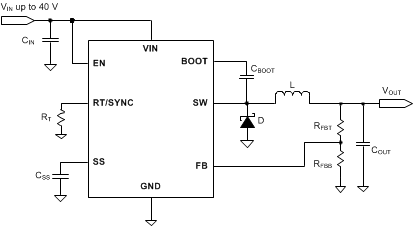
 Simplified Schematic
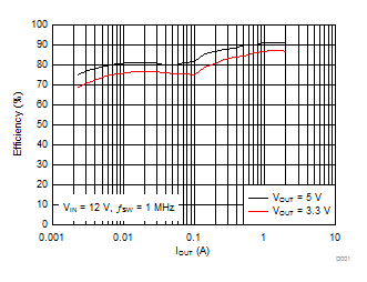
 Efficiency vs Output Current