SNVSA81A February 2015 – April 2015 LMR14030
PRODUCTION DATA.
- 1 Features
- 2 Applications
- 3 Description
- 4 Simplified Schematic
- 5 Revision History
- 6 Pin Configuration and Functions
- 7 Specifications
-
8 Detailed Description
- 8.1 Overview
- 8.2 Functional Block Diagram
- 8.3
Feature Description
- 8.3.1 Fixed Frequency Peak Current Mode Control
- 8.3.2 Slope Compensation
- 8.3.3 Sleep-mode
- 8.3.4 Low Dropout Operation and Bootstrap Voltage (BOOT)
- 8.3.5 Adjustable Output Voltage
- 8.3.6 Enable and Adjustable Under-voltage Lockout
- 8.3.7 External Soft-start
- 8.3.8 Switching Frequency and Synchronization (RT/SYNC)
- 8.3.9 Over Current and Short Circuit Protection
- 8.3.10 Overvoltage Protection
- 8.3.11 Thermal Shutdown
- 9 Application and Implementation
- 10Power Supply Recommendations
- 11Layout
- 12Device and Documentation Support
- 13Mechanical, Packaging, and Orderable Information
パッケージ・オプション
メカニカル・データ(パッケージ|ピン)
- DDA|8
サーマルパッド・メカニカル・データ
- DDA|8
発注情報
9 Application and Implementation
NOTE
Information in the following applications sections is not part of the TI component specification, and TI does not warrant its accuracy or completeness. TI’s customers are responsible for determining suitability of components for their purposes. Customers should validate and test their design implementation to confirm system functionality.
9.1 Application Information
The LMR14030 is a step down DC-to-DC regulator. It is typically used to convert a higher DC voltage to a lower DC voltage with a maximum output current of 3.5 A. The following design procedure can be used to select components for the LMR14030. This section presents a simplified discussion of the design process.
9.2 Typical Application
The LMR14030 only requires a few external components to convert from wide voltage range supply to a fixed output voltage. A schematic of 5 V/3.5 A application circuit is shown in Figure 21. The external components have to fulfill the needs of the application, but also the stability criteria of the device’s control loop.
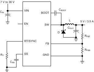 Figure 21. Application Circuit, 5V Output
9.2.1 Design Requirements
This example details the design of a high frequency switching regulator using ceramic output capacitors. A few parameters must be known in order to start the design process. These parameters are typically determined at the system level:
| Input Voltage, VIN | 7 V to 36 V, Typical 12 V |
| Output Voltage, VOUT | 5.0 V |
| Maximum Output Current IO_MAX | 3.5 A |
| Transient Response 0.35 A to 3.5 A | 5% |
| Output Voltage Ripple | 50 mV |
| Input Voltage Ripple | 400 mV |
| Switching Frequency fSW | 500 kHz |
| Soft-start time | 5 ms |
9.2.2 Detailed Design Procedure
9.2.2.1 Output Voltage Set-Point
The output voltage of LMR14030 is externally adjustable using a resistor divider network. The divider network is comprised of top feedback resistor RFBT and bottom feedback resistor RFBB. Equation 7 is used to determine the output voltage:

Choose the value of RFBT to be 100 kΩ. With the desired output voltage set to 5 V and the VFB = 0.75 V, the RFBB value can then be calculated using Equation 7. The formula yields to a value 17.65 kΩ. Choose the closest available value of 17.8 kΩ for RFBB.
9.2.2.2 Switching Frequency
For desired frequency, use Equation 8 to calculate the required value for RT.

For 500 kHz, the calculated RT is 49.2 kΩ and standard value 49.9 kΩ can be used to set the switching frequency at 500 kHz.
9.2.2.3 Output Inductor Selection
The most critical parameters for the inductor are the inductance, saturation current and the RMS current. The inductance is based on the desired peak-to-peak ripple current ΔiL. Since the ripple current increases with the input voltage, the maximum input voltage is always used to calculate the minimum inductance LMIN. Use Equation 10 to calculate the minimum value of the output inductor. KIND is a coefficient that represents the amount of inductor ripple current relative to the maximum output current. A reasonable value of KIND should be 20%-40%. During an instantaneous short or over current operation event, the RMS and peak inductor current can be high. The inductor current rating should be higher than current limit.


In general, it is preferable to choose lower inductance in switching power supplies, because it usually corresponds to faster transient response, smaller DCR, and reduced size for more compact designs. But too low of an inductance can generate too large of an inductor current ripple such that over current protection at the full load could be falsely trigged. It also generates more conduction loss since the RMS current is slightly higher. Larger inductor current ripple also implies larger output voltage ripple with same output capacitors. With peak current mode control, it is not recommended to have too small of an inductor current ripple. A larger peak current ripple improves the comparator signal to noise ratio.
For this design example, choose KIND = 0.4, the minimum inductor value is calculated to be 6.12 µH, and a nearest standard value is chosen: 6.5 µH. A standard 6.5 μH ferrite inductor with a capability of 5 A RMS current and 7A saturation current can be used.
9.2.2.4 Output Capacitor Selection
The output capacitor(s), COUT, should be chosen with care since it directly affects the steady state output voltage ripple, loop stability and the voltage over/undershoot during load current transients.
The output ripple is essentially composed of two parts. One is caused by the inductor current ripple going through the Equivalent Series Resistance (ESR) of the output capacitors:

The other is caused by the inductor current ripple charging and discharging the output capacitors:

The two components in the voltage ripple are not in phase, so the actual peak-to-peak ripple is smaller than the sum of two peaks.
Output capacitance is usually limited by transient performance specifications if the system requires tight voltage regulation with presence of large current steps and fast slew rate. When a fast large load increase happens, output capacitors provide the required charge before the inductor current can slew up to the appropriate level. The regulator’s control loop usually needs three or more clock cycles to respond to the output voltage droop. The output capacitance must be large enough to supply the current difference for three clock cycles to maintain the output voltage within the specified range. Equation 13
Equation 13 shows the minimum output capacitance needed for specified output undershoot. When a sudden large load decrease happens, the output capacitors absorb energy stored in the inductor. The catch diode can’t sink current so the energy stored in the inductor results in an output voltage overshoot. Equation 14 calculates the minimum capacitance required to keep the voltage overshoot within a specified range.


where
- KIND = Ripple ratio of the inductor ripple current (ΔiL / IOUT)
- IOL = Low level output current during load transient
- IOH = High level output current during load transient
- VUS = Target output voltage undershoot
- VOS = Target output voltage overshoot
For this design example, the target output ripple is 50 mV. Presuppose ΔVOUT_ESR = ΔVOUT_C = 50 mV, and chose KIND = 0.4. Equation 11 yields ESR no larger than 35.7 mΩ and Equation 12 yields COUT no smaller than 7 μF. For the target over/undershoot range of this design, VUS = VOS = 5% × VOUT = 250 mV. The COUT can be calculated to be no smaller than 75.6 μF and 30.8 μF by Equation 13 and Equation 14 respectively. In summary, the most stringent criteria for the output capacitor is 75.6 μF. Two 47 μF, 16 V, X7R ceramic capacitors with 5 mΩ ESR are used in parallel.
9.2.2.5 Schottky Diode Selection
The breakdown voltage rating of the diode is preferred to be 25% higher than the maximum input voltage. The current rating for the diode should be equal to the maximum output current for best reliability in most applications. In cases where the input voltage is much greater than the output voltage the average diode current is lower. In this case it is possible to use a diode with a lower average current rating, approximately (1-D) × IOUT however the peak current rating should be higher than the maximum load current. A 4 A to 5 A rated diode is a good starting point.
9.2.2.6 Input Capacitor Selection
The LMR14030 device requires high frequency input decoupling capacitor(s) and a bulk input capacitor, depending on the application. The typical recommended value for the high frequency decoupling capacitor is 4.7 μF to 10 μF. A high-quality ceramic capacitor type X5R or X7R with sufficiency voltage rating is recommended. To compensate the derating of ceramic capacitors, a voltage rating of twice the maximum input voltage is recommended. Additionally, some bulk capacitance can be required, especially if the LMR14030 circuit is not located within approximately 5 cm from the input voltage source. This capacitor is used to provide damping to the voltage spike due to the lead inductance of the cable or the trace. For this design, two 2.2 μF, X7R ceramic capacitors rated for 100 V are used. A 0.1 μF for high-frequency filtering and place it as close as possible to the device pins.
9.2.2.7 Bootstrap Capacitor Selection
Every LMR14030 design requires a bootstrap capacitor (CBOOT). The recommended capacitor is 0.1 μF and rated 16 V or higher. The bootstrap capacitor is located between the SW pin and the BOOT pin. The bootstrap capacitor must be a high-quality ceramic type with an X7R or X5R grade dielectric for temperature stability.
9.2.2.8 Soft-start Capacitor Selection
Use Equation 15 in order to calculate the soft-start capacitor value:

where
- CSS = Soft-start capacitor value
- ISS = Soft-start charging current (3 μA)
- tSS = Desired soft-start time
For the desired soft-start time of 5 ms and soft-start charging current of 3.0 μA, Equation 15 yields a soft-start capacitor value of 20 nF, a standard 22 nF ceramic capacitor is used.
9.2.3 Application Curves
Unless otherwise specified the following conditions apply: VIN = 12 V, fSW = 500 kHz, L = 5.6 µH, COUT = 47 µF x 2, TA = 25°C.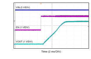
| VIN = 12 V | VOUT = 5 V | IOUT = 2 A |
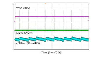
| VIN = 12 V | VOUT = 5 V | IOUT = 0 A |
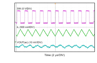
| VIN = 12 V | VOUT = 5 V | IOUT = 1.5 A |
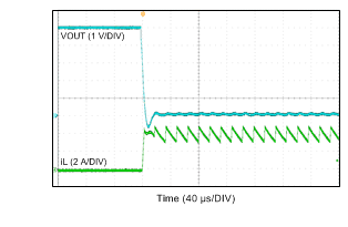
| VIN = 12 V | VOUT = 5 V |
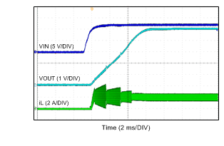
| VIN = 12 V | VOUT = 5 V | IOUT = 2 A |
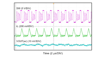
| VIN = 12 V | VOUT = 5 V | IOUT = 100 mA |
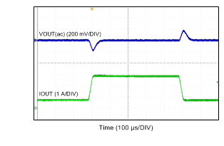
| IOUT: 20% → 80% of 3.5 A | Slew rate = 100 mA/μs |
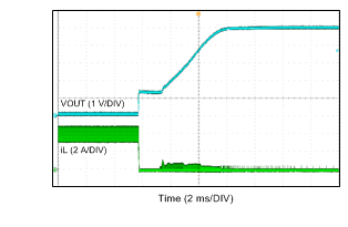
| VIN = 12 V | VOUT = 5 V |