-
LMR16020 SIMPLE SWITCHER® 60 V, 2 A Step-Down Converter With 40 µA IQ
- 1 Features
- 2 Applications
- 3 Description
- 4 Revision History
- 5 Pin Configuration and Functions
- 6 Specifications
-
7 Detailed Description
- 7.1 Overview
- 7.2 Functional Block Diagram
- 7.3
Feature Description
- 7.3.1 Fixed Frequency Peak Current Mode Control
- 7.3.2 Slope Compensation
- 7.3.3 Sleep-mode
- 7.3.4 Low Dropout Operation and Bootstrap Voltage (BOOT)
- 7.3.5 Adjustable Output Voltage
- 7.3.6 Enable and Adjustable Under-voltage Lockout
- 7.3.7 Switching Frequency and Synchronization (RT/SYNC)
- 7.3.8 Power Good (PGOOD)
- 7.3.9 Over Current and Short Circuit Protection
- 7.3.10 Overvoltage Protection
- 7.3.11 Thermal Shutdown
- 7.4 Device Functional Modes
- 8 Application and Implementation
- 9 Power Supply Recommendations
- 10Layout
- 11Device and Documentation Support
- 12Mechanical, Packaging, and Orderable Information
- IMPORTANT NOTICE
パッケージ・オプション
メカニカル・データ(パッケージ|ピン)
- DDA|8
サーマルパッド・メカニカル・データ
- DDA|8
発注情報
LMR16020 SIMPLE SWITCHER® 60 V, 2 A Step-Down Converter With 40 µA IQ
1 Features
- 4.3 V to 60 V Input Range
- 2 A Continuous Output Current
- Ultra-low 40 µA Operating Quiescent Current
- 155 mΩ High-Side MOSFET
- Current Mode Control
- Adjustable Switching Frequency from 200 kHz to 2.5 MHz
- Frequency Synchronization to External Clock
- Internal Compensation for Ease of Use
- High Duty Cycle Operation Supported
- Precision Enable Input
- Power-Good Flag
- 1 µA Shutdown Current
- Thermal, Overvoltage and Short Protection
- 8-Pin HSOIC with PowerPAD™ Package
2 Applications
- Automotive Battery Regulation
- Industrial Power Supplies
- Telecom and Datacom Systems
- General Purpose Wide Vin Regulation
space
3 Description
The LMR16020 is a 60 V, 2 A SIMPLE SWITCHER® step down regulator with an integrated high-side MOSFET. With a wide input range from 4.3 V to 60 V, it’s suitable for various applications from industrial to automotive for power conditioning from unregulated sources. The regulator’s quiescent current is 40 µA in Sleep-mode, which is suitable for battery powered systems. An ultra-low 1 μA current in shutdown mode can further prolong battery life. A wide adjustable switching frequency range allows either efficiency or external component size to be optimized. Internal loop compensation means that the user is free from the tedious task of loop compensation design. This also minimizes the external components of the device. A precision enable input allows simplification of regulator control and system power sequencing. The device also has built-in protection features such as cycle-by-cycle current limit, thermal sensing and shutdown due to excessive power dissipation, and output overvoltage protection.
The LMR16020 is available in an 8-pin HSOIC package with exposed pad for low thermal resistance.
Device Information (1)
| PART NUMBER | PACKAGE | BODY SIZE (NOM) |
|---|---|---|
| LMR16020PDDAR | HSOIC (8) | 4.89 mm x 3.90 mm |
- For all available packages, see the orderable addendum at the end of the datasheet.
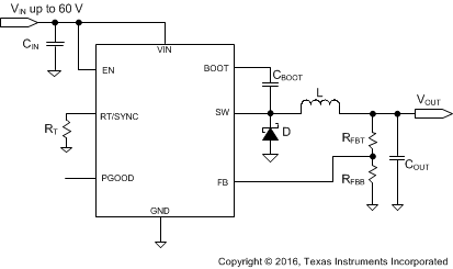
Simplified Schematic

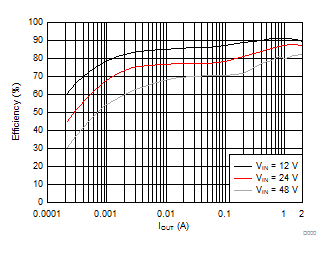
Efficiency vs Output Current
Vout = 5 V, fsw = 500 kHz

4 Revision History
Changes from * Revision (December 2015) to A Revision
- Changed from Product Preview to Production Data with full version of the datasheetGo
5 Pin Configuration and Functions

Pin Functions
| PIN | TYPE (1) | DESCRIPTION | |
|---|---|---|---|
| NAME | NO. | ||
| BOOT | 1 | P | Bootstrap capacitor connection for high-side MOSFET driver. Connect a high quality 0.1 μF capacitor from BOOT to SW. |
| VIN | 2 | P | Connect to power supply and bypass capacitors CIN. Path from VIN pin to high frequency bypass CIN and GND must be as short as possible. |
| EN | 3 | A | Enable pin, with internal pull-up current source. Pull below 1.2 V to disable. Float or connect to VIN to enable. Adjust the input under voltage lockout with two resistors. See the Enable and Adjusting Under voltage lockout section. |
| RT/SYNC | 4 | A | Resistor Timing or External Clock input. An internal amplifier holds this pin at a fixed voltage when using an external resistor to ground to set the switching frequency. If the pin is pulled above the PLL upper threshold, a mode change occurs and the pin becomes a synchronization input. The internal amplifier is disabled and the pin is a high impedance clock input to the internal PLL. If clocking edges stop, the internal amplifier is re-enabled and the operating mode returns to frequency programming by resistor. |
| FB | 5 | A | Feedback input pin, connect to the feedback divider to set VOUT. Do not short this pin to ground during operation. |
| PGOOD | 6 | A | Power-Good pin, open drain output for power-good flag, use a 10 kΩ to 100 kΩ pull-up resistor to logic rail or other DC voltage no higher than 7 V. |
| GND | 7 | G | System ground pin. |
| SW | 8 | P | Switching output of the regulator. Internally connected to high-side power MOSFET. Connect to power inductor. |
| Thermal Pad | 9 | G | Major heat dissipation path of the die. Must be connected to ground plane on PCB. |