JAJSCV3A December 2016 – April 2017 LMR23610-Q1
PRODUCTION DATA.
- 1 特長
- 2 アプリケーション
- 3 概要
- 4 改訂履歴
- 5 Pin Configuration and Functions
- 6 Specifications
-
7 Detailed Description
- 7.1 Overview
- 7.2 Functional Block Diagram
- 7.3
Feature Description
- 7.3.1 Fixed Frequency Peak Current Mode Control
- 7.3.2 Adjustable Output Voltage
- 7.3.3 Enable/Sync
- 7.3.4 VCC, UVLO
- 7.3.5 Minimum ON-time, Minimum OFF-time and Frequency Foldback at Drop-out Conditions
- 7.3.6 Internal Compensation and CFF
- 7.3.7 Bootstrap Voltage (BOOT)
- 7.3.8 Over Current and Short Circuit Protection
- 7.3.9 Thermal Shutdown
- 7.4 Device Functional Modes
-
8 Application and Implementation
- 8.1 Application Information
- 8.2
Typical Applications
- 8.2.1 Design Requirements
- 8.2.2
Detailed Design Procedure
- 8.2.2.1 Custom Design With WEBENCH® Tools
- 8.2.2.2 Output Voltage Set-Point
- 8.2.2.3 Switching Frequency
- 8.2.2.4 Inductor Selection
- 8.2.2.5 Output Capacitor Selection
- 8.2.2.6 Feed-Forward Capacitor
- 8.2.2.7 Input Capacitor Selection
- 8.2.2.8 Bootstrap Capacitor Selection
- 8.2.2.9 VCC Capacitor Selection
- 8.2.2.10 Under Voltage Lockout Set-Point
- 8.2.3 Application Curves
- 9 Power Supply Recommendations
- 10Layout
- 11デバイスおよびドキュメントのサポート
- 12メカニカル、パッケージ、および注文情報
パッケージ・オプション
メカニカル・データ(パッケージ|ピン)
- DDA|8
サーマルパッド・メカニカル・データ
- DDA|8
発注情報
6 Specifications
6.1 Absolute Maximum Ratings
Over the recommended operating junction temperature range of -40 °C to 125 °C (unless otherwise noted) (1)| PARAMETER | MIN | MAX | UNIT | |
|---|---|---|---|---|
| Input Voltages | VIN to PGND | -0.3 | 42 | V |
| EN/SYNC to AGND | -5.5 | VIN + 0.3 | ||
| FB to AGND | -0.3 | 4.5 | ||
| AGND to PGND | -0.3 | 0.3 | ||
| Output Voltages | SW to PGND | -1 | VIN + 0.3 | V |
| SW to PGND less than 10 ns transients | -5 | 42 | ||
| BOOT to SW | -0.3 | 5.5 | ||
| VCC to AGND | -0.3 | 4.5 (2) | ||
| TJ | Junction temperature | -40 | 150 | °C |
| Tstg | Storage temperature | -65 | 150 | °C |
(1) Stresses beyond those listed under Absolute Maximum Ratings may cause permanent damage to the device. These are stress ratings only, which do not imply functional operation of the device at these or any other conditions beyond those indicated under Recommended Operating Conditions. Exposure to absolute-maximum-rated conditions for extended periods may affect device reliability.
(2) In shutdown mode, the VCC to AGND maximum value is 5.25 V.
6.2 ESD Ratings
| VALUE | UNIT | |||
|---|---|---|---|---|
| V(ESD) | Electrostatic discharge | Human-body model (HBM) (1) | ±2000 | V |
| Charged-device model (CDM) | ±1000 | |||
(1) AEC Q100-002 indicates that HBM stressing shall be in accordance with the ANSI/ESDA/JEDEC JS-001 specification.
6.3 Recommended Operating Conditions
Over the recommended operating junction temperature range of -40 °C to 125 °C (unless otherwise noted) (1)| MIN | MAX | UNIT | ||
|---|---|---|---|---|
| Input Voltage | VIN | 4 | 36 | V |
| EN/SYNC | -5 | 36 | ||
| FB | -0.3 | 1.2 | ||
| Output Voltage | VOUT | 1 | 28 | V |
| Output Current | IOUT | 0 | 1 | A |
| Temperature | Operating junction temperature, TJ | -40 | 125 | °C |
(1) Operating Ratings indicate conditions for which the device is intended to be functional, but do not guarantee specific performance limits. For guaranteed specifications, see Electrical Characteristics.
6.4 Thermal Information
| THERMAL METRIC (1) (2) | DDA (8 PINS) | UNIT | |
|---|---|---|---|
| RθJA | Junction-to-ambient thermal resistance | 42.0 | °C/W |
| ψJT | Junction-to-top characterization parameter | 5.9 | |
| ψJB | Junction-to-board characterization parameter | 23.4 | |
| RθJC(top) | Junction-to-case (top) thermal resistance | 45.8 | |
| RθJC(bot) | Junction-to-case (bottom) thermal resistance | 3.6 | |
| RθJB | Junction-to-board thermal resistance | 23.4 | |
(1) For more information about traditional and new thermal metrics, see the Semiconductor and IC Package Thermal Metrics application report, SPRA953.
(2) Power rating at a specific ambient temperature TA should be determined with a maximum junction temperature (TJ) of 125 °C, which is illustrated in Recommended Operating Conditions section.
6.5 Electrical Characteristics
Limits apply over the recommended operating junction temperature (TJ) range of -40 °C to +125 °C, unless otherwise stated. Minimum and Maximum limits are specified through test, design or statistical correlation. Typical values represent the most likely parametric norm at TJ = 25 °C, and are provided for reference purposes only.| PARAMETER | TEST CONDITIONS | MIN | TYP | MAX | UNIT | |
|---|---|---|---|---|---|---|
| POWER SUPPLY (VIN PIN) | ||||||
| VIN | Operation input voltage | 4 | 36 | V | ||
| VIN_UVLO | Under voltage lockout thresholds | Rising threshold | 3.3 | 3.7 | 3.9 | V |
| Falling threshold | 2.9 | 3.3 | 3.5 | |||
| ISHDN | Shutdown supply current | VEN = 0 V, VIN = 12 V, TJ = -40 °C to 125 °C | 2.0 | 4.0 | μA | |
| IQ | Operating quiescent current (non- switching) | VIN =12 V, VFB = 1.1 V, TJ = -40 °C to 125 °C, PFM mode | 75 | μA | ||
| ENABLE (EN PIN) | ||||||
| VEN_H | Enable rising threshold Voltage | 1.4 | 1.55 | 1.7 | V | |
| VEN_HYS | Enable hysteresis voltage | 0.4 | V | |||
| VWAKE | Wake-up threshold | 0.4 | V | |||
| IEN | Input leakage current at EN pin | VIN = 4 V to 36 V, VEN= 2 V | 10 | 100 | nA | |
| VIN = 4 V to 36 V, VEN= 36 V | 1 | μA | ||||
| VOLTAGE REFERENCE (FB PIN) | ||||||
| VREF | Reference voltage | VIN = 4 V to 36 V, TJ = 25 °C | 0.985 | 1.0 | 1.015 | V |
| VIN = 4 V to 36 V, TJ = -40 °C to 125 °C | 0.980 | 1.0 | 1.020 | |||
| ILKG_FB | Input leakage current at FB pin | VFB= 1 V | 10 | nA | ||
| INTERNAL LDO (VCC PIN) | ||||||
| VCC | Internal LDO output voltage | 4.1 | V | |||
| VCC_UVLO | VCC under voltage lockout thresholds | Rising threshold | 2.8 | 3.2 | 3.6 | V |
| Falling threshold | 2.4 | 2.8 | 3.2 | |||
| CURRENT LIMIT | ||||||
| IHS_LIMIT | Peak inductor current limit | 1.4 | 2.0 | 2.6 | A | |
| ILS_LIMIT | Valley inductor current limit | 1.0 | 1.5 | 2.1 | A | |
| IL_ZC | Zero cross current limit | -0.04 | A | |||
| INTEGRATED MOSFETS | ||||||
| RDS_ON_HS | High-side MOSFET ON-resistance | VIN = 12 V, IOUT = 1 A | 185 | mΩ | ||
| RDS_ON_LS | Low-side MOSFET ON-resistance | VIN = 12 V, IOUT = 1 A | 105 | mΩ | ||
| THERMAL SHUTDOWN | ||||||
| TSHDN | Thermal shutdown threshold | 162 | 170 | 178 | °C | |
| THYS | Hysteresis | 15 | °C | |||
6.6 Timing Characteristics
Over the recommended operating junction temperature range of -40 °C to 125 °C (unless otherwise noted)| PARAMETER | TEST CONDITIONS | MIN | TYP | MAX | UNIT | |
|---|---|---|---|---|---|---|
| HICCUP MODE | ||||||
| NOC(1) | Number of cycles that LS current limit is tripped to enter Hiccup mode | 64 | Cycles | |||
| TOC | Hiccup retry delay time | 5 | ms | |||
| SOFT START | ||||||
| TSS | Internal soft-start time | The time of internal reference to increase from 0 V to 1.0 V | 1 | 2 | 3 | ms |
(1) Guaranteed by design.
6.7 Switching Characteristics
Over the recommended operating junction temperature range of -40 °C to 125 °C (unless otherwise noted)| PARAMETER | MIN | TYP | MAX | UNIT | ||
|---|---|---|---|---|---|---|
| SW (SW PIN) | ||||||
| fSW | Default switching frequency | 340 | 400 | 460 | kHz | |
| TON_MIN | Minimum turn-on time | 60 | 90 | ns | ||
| TOFF_MIN(1) | Minimum turn-off time | 100 | ns | |||
| SYNC (EN/SYNC PIN) | ||||||
| fSYNC | SYNC frequency range | 200 | 2200 | kHz | ||
| VSYNC | Amplitude of SYNC clock AC signal (measured at SYNC pin) | 2.8 | 5.5 | V | ||
| TSYNC_MIN | Minimum sync clock ON and OFF time | 100 | ns | |||
(1) Guaranteed by design.
6.8 Typical Characteristics
Unless otherwise specified the following conditions apply: VIN = 12 V, fSW = 400 kHz, L = 22 µH, COUT = 47 µF × 2, TA = 25°C.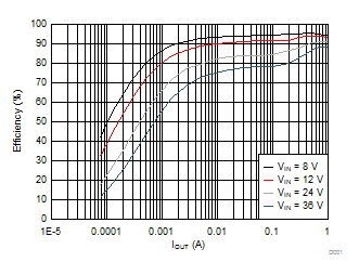
| fSW = 400 kHz | VOUT = 5 V |
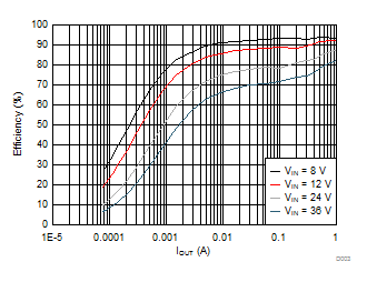
| fSW = 1000 kHz (Sync) | VOUT = 5 V |
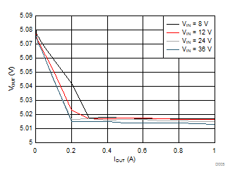
| VOUT = 5 V |
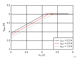
| VOUT = 5 V |
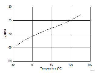
| VIN = 12 V | VFB = 1.1 V |
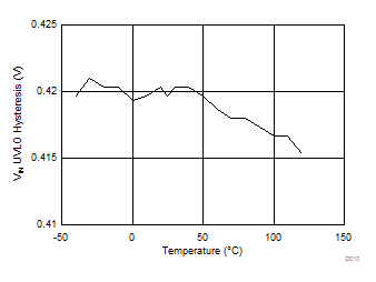
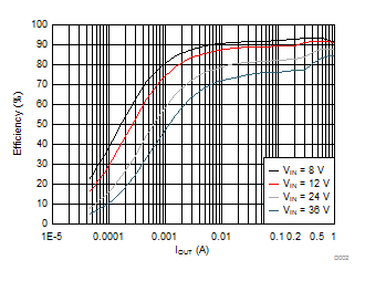
| fSW = 400 kHz | VOUT = 3.3 V |
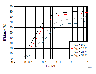
| fSW = 1000 kHz (Sync) | VOUT = 3.3 V |
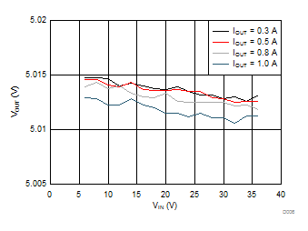
| VOUT = 5 V |
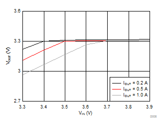
| VOUT = 3.3 V |
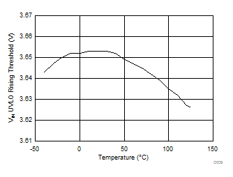
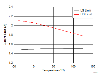
| VIN = 12 V |