JAJSCV3A December 2016 – April 2017 LMR23610-Q1
PRODUCTION DATA.
- 1 特長
- 2 アプリケーション
- 3 概要
- 4 改訂履歴
- 5 Pin Configuration and Functions
- 6 Specifications
-
7 Detailed Description
- 7.1 Overview
- 7.2 Functional Block Diagram
- 7.3
Feature Description
- 7.3.1 Fixed Frequency Peak Current Mode Control
- 7.3.2 Adjustable Output Voltage
- 7.3.3 Enable/Sync
- 7.3.4 VCC, UVLO
- 7.3.5 Minimum ON-time, Minimum OFF-time and Frequency Foldback at Drop-out Conditions
- 7.3.6 Internal Compensation and CFF
- 7.3.7 Bootstrap Voltage (BOOT)
- 7.3.8 Over Current and Short Circuit Protection
- 7.3.9 Thermal Shutdown
- 7.4 Device Functional Modes
-
8 Application and Implementation
- 8.1 Application Information
- 8.2
Typical Applications
- 8.2.1 Design Requirements
- 8.2.2
Detailed Design Procedure
- 8.2.2.1 Custom Design With WEBENCH® Tools
- 8.2.2.2 Output Voltage Set-Point
- 8.2.2.3 Switching Frequency
- 8.2.2.4 Inductor Selection
- 8.2.2.5 Output Capacitor Selection
- 8.2.2.6 Feed-Forward Capacitor
- 8.2.2.7 Input Capacitor Selection
- 8.2.2.8 Bootstrap Capacitor Selection
- 8.2.2.9 VCC Capacitor Selection
- 8.2.2.10 Under Voltage Lockout Set-Point
- 8.2.3 Application Curves
- 9 Power Supply Recommendations
- 10Layout
- 11デバイスおよびドキュメントのサポート
- 12メカニカル、パッケージ、および注文情報
パッケージ・オプション
メカニカル・データ(パッケージ|ピン)
- DDA|8
サーマルパッド・メカニカル・データ
- DDA|8
発注情報
8 Application and Implementation
NOTE
Information in the following applications sections is not part of the TI component specification, and TI does not warrant its accuracy or completeness. TI’s customers are responsible for determining suitability of components for their purposes. Customers should validate and test their design implementation to confirm system functionality.
8.1 Application Information
The LMR23610-Q1 is a step down DC-to-DC regulator. It is typically used to convert a higher DC voltage to a lower DC voltage with a maximum output current of 1 A. The following design procedure can be used to select components for the LMR23610-Q1. Alternately, the WEBENCH® software may be used to generate complete designs. When generating a design, the WEBENCH® software utilizes iterative design procedure and accesses comprehensive databases of components. Please go to ti.com for more details.
8.2 Typical Applications
The LMR23610-Q1 only requires a few external components to convert from a wide voltage range supply to a fixed output voltage. Figure 21 shows a basic schematic.
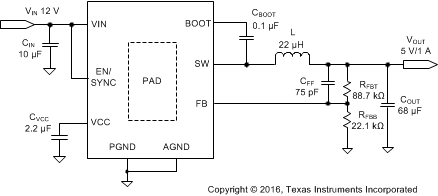 Figure 21. Application Circuit
The external components have to fulfill the needs of the application, but also the stability criteria of the device's control loop. Table 1 can be used to simplify the output filter component selection.
Table 1. L, COUT and CFF Typical Values
| fSW (kHz) | VOUT (V) | L (µH) | COUT (µF) | CFF (pF) | RFBT (kΩ) |
|---|---|---|---|---|---|
| 400 | 3.3 | 15 | 82 | 100 | 51 |
| 400 | 5 | 22 | 68 | 75 | 88.7 |
| 400 | 12 | 47 | 33 | See note (5) | 243 |
| 400 | 24 | 47 | 22 | See note (5) | 510 |
- Inductance value is calculated based on VIN = 36 V.
- All the COUT values are after derating. Add more when using ceramic capacitors.
- RFBT = 0 Ω for VOUT = 1 V. RFBB = 22.1 kΩ for all other VOUT setting.
- For designs with RFBT other than recommended value, please adjust CFF such that (CFF × RFBT) is unchanged and adjust RFBB such that (RFBT / RFBB) is unchanged.
- High ESR COUT will give enough phase boost and CFF not needed.
8.2.1 Design Requirements
Detailed design procedure is described based on a design example. For this design example, use the parameters listed in Table 2 as the input parameters.
Table 2. Design Example Parameters
| Input Voltage, VIN | 12 V typical, range from 8 V to 28 V |
| Output Voltage, VOUT | 5 V |
| Maximum Output Current IO_MAX | 1 A |
| Transient Response 0.1 A to 1 A | 5% |
| Output Voltage Ripple | 50 mV |
| Input Voltage Ripple | 400 mV |
| Switching Frequency fSW | 400 kHz |
8.2.2 Detailed Design Procedure
8.2.2.1 Custom Design With WEBENCH® Tools
Click here to create a custom design using the LMR23610-Q1 device with the WEBENCH® Power Designer.
- Start by entering the input voltage (VIN), output voltage (VOUT), and output current (IOUT) requirements.
- Optimize the design for key parameters such as efficiency, footprint, and cost using the optimizer dial.
- Compare the generated design with other possible solutions from Texas Instruments.
The WEBENCH Power Designer provides a customized schematic along with a list of materials with real-time pricing and component availability.
In most cases, these actions are available:
- Run electrical simulations to see important waveforms and circuit performance
- Run thermal simulations to understand board thermal performance
- Export customized schematic and layout into popular CAD formats
- Print PDF reports for the design, and share the design with colleagues
Get more information about WEBENCH tools at www.ti.com/WEBENCH.
8.2.2.2 Output Voltage Set-Point
The output voltage of LMR23610-Q1 is externally adjustable using a resistor divider network. The divider network is comprised of top feedback resistor RFBT and bottom feedback resistor RFBB. Equation 10 is used to determine the output voltage:

Choose the value of RFBB to be 22.1 kΩ. With the desired output voltage set to 5 V and the VREF = 1.0 V, the RFBB value can then be calculated using Equation 10. The formula yields to a value 88.7 kΩ.
8.2.2.3 Switching Frequency
The default switching frequency of the LMR23610-Q1 is 400 kHz. For other switching frequency, the device must be synchronized to an external clock, please refer to Enable/Sync for more details.
8.2.2.4 Inductor Selection
The most critical parameters for the inductor are the inductance, saturation current and the rated current. The inductance is based on the desired peak-to-peak ripple current ΔiL. Since the ripple current increases with the input voltage, the maximum input voltage is always used to calculate the minimum inductance LMIN. Use Equation 12 to calculate the minimum value of the output inductor. KIND is a coefficient that represents the amount of inductor ripple current relative to the maximum output current of the device. A reasonable value of KIND should be 30% to 50%. During an instantaneous short or over current operation event, the RMS and peak inductor current can be high. The inductor current rating should be higher than the current limit of the device.


In general, it is preferable to choose lower inductance in switching power supplies, because it usually corresponds to faster transient response, smaller DCR, and reduced size for more compact designs. But too low of an inductance can generate too large of an inductor current ripple such that over current protection at the full load could be falsely triggered. It also generates more conduction loss and inductor core loss. Larger inductor current ripple also implies larger output voltage ripple with same output capacitors. With peak current mode control, it is not recommended to have too small of an inductor current ripple. A larger peak current ripple improves the comparator signal to noise ratio.
For this design example, choose KIND = 0.5, the minimum inductor value is calculated to be 20.5 µH. Choose the nearest standard 22 μH ferrite inductor with a capability of 2 A RMS current and 2.5 A saturation current.
8.2.2.5 Output Capacitor Selection
The output capacitor(s), COUT, should be chosen with care since it directly affects the steady state output voltage ripple, loop stability and the voltage over/undershoot during load current transients.
The output ripple is essentially composed of two parts. One is caused by the inductor current ripple going through the Equivalent Series Resistance (ESR) of the output capacitors:

The other is caused by the inductor current ripple charging and discharging the output capacitors:

The two components in the voltage ripple are not in phase, so the actual peak-to-peak ripple is smaller than the sum of two peaks.
Output capacitance is usually limited by transient performance specifications if the system requires tight voltage regulation with presence of large current steps and fast slew rate. When a fast large load increase happens, output capacitors provide the required charge before the inductor current can slew up to the appropriate level. The regulator’s control loop usually needs six or more clock cycles to respond to the output voltage droop. The output capacitance must be large enough to supply the current difference for six clock cycles to maintain the output voltage within the specified range. Equation 15 shows the minimum output capacitance needed for specified output undershoot. When a sudden large load decrease happens, the output capacitors absorb energy stored in the inductor. which results in an output voltage overshoot. Equation 16 calculates the minimum capacitance required to keep the voltage overshoot within a specified range.


where
- KIND = Ripple ratio of the inductor ripple current (ΔiL / IOUT)
- IOL = Low level output current during load transient
- IOH = High level output current during load transient
- VUS = Target output voltage undershoot
- VOS = Target output voltage overshoot
For this design example, the target output ripple is 50 mV. Presuppose ΔVOUT_ESR = ΔVOUT_C = 50 mV, and chose KIND = 0.5. Equation 13 yields ESR no larger than 100 mΩ and Equation 14 yields COUT no smaller than 3.1 μF. For the target over/undershoot range of this design, VUS = VOS = 5% × VOUT = 250 mV. The COUT can be calculated to be no smaller than 54 μF and 8.5 μF by Equation 15 and Equation 16 respectively. Consider of derating, one 82 μF, 16 V ceramic capacitor with 5 mΩ ESR is used.
8.2.2.6 Feed-Forward Capacitor
The LMR23610-Q1 is internally compensated. Depending on the VOUT and frequency fSW, if the output capacitor COUT is dominated by low ESR (ceramic types) capacitors, it could result in low phase margin. To improve the phase boost an external feedforward capacitor CFF can be added in parallel with RFBT. CFF is chosen such that phase margin is boosted at the crossover frequency without CFF. A simple estimation for the crossover frequency (fX) without CFF is shown in Equation 17, assuming COUT has very small ESR, and COUT value is after derating.

The following equation for CFF was tested:

For designs with higher ESR, CFF is not needed when COUT has very high ESR and CFF calculated from Equation 18 should be reduced with medium ESR. Table 1 can be used as a quick starting point.
For the application in this design example, a 75 pF, 50 V, COG capacitor is selected.
8.2.2.7 Input Capacitor Selection
The LMR23610-Q1 device requires high frequency input decoupling capacitor(s) and a bulk input capacitor, depending on the application. The typical recommended value for the high frequency decoupling capacitor is 4.7 μF to 10 μF. A high-quality ceramic capacitor type X5R or X7R with sufficiency voltage rating is recommended. To compensate the derating of ceramic capacitors, a voltage rating of twice the maximum input voltage is recommended. Additionally, some bulk capacitance can be required, especially if the LMR23610-Q1 circuit is not located within approximately 5 cm from the input voltage source. This capacitor is used to provide damping to the voltage spike due to the lead inductance of the cable or the trace. For this design, two 4.7 μF, 50 V, X7R ceramic capacitors are used. A 0.1 μF for high-frequency filtering and place it as close as possible to the device pins.
8.2.2.8 Bootstrap Capacitor Selection
Every LMR23610-Q1 design requires a bootstrap capacitor (CBOOT). The recommended capacitor is 0.1 μF and rated 16 V or higher. The bootstrap capacitor is located between the SW pin and the BOOT pin. The bootstrap capacitor must be a high-quality ceramic type with an X7R or X5R grade dielectric for temperature stability.
8.2.2.9 VCC Capacitor Selection
The VCC pin is the output of an internal LDO for LMR23610-Q1. To insure stability of the device, place a minimum of 2.2 μF, 16 V, X7R capacitor from this pin to ground.
8.2.2.10 Under Voltage Lockout Set-Point
The system undervoltage lockout (UVLO) is adjusted using the external voltage divider network of RENT and RENB. The UVLO has two thresholds, one for power up when the input voltage is rising and one for power down or brown outs when the input voltage is falling. The following equation can be used to determine the VIN UVLO level.

The EN rising threshold (VENH) for LMR23610-Q1 is set to be 1.55 V (typ). Choose the value of RENB to be 287 kΩ to minimize input current from the supply. If the desired VIN UVLO level is at 6.0 V, then the value of RENT can be calculated using the equation below:

The above equation yields a value of 820 kΩ. The resulting falling UVLO threshold, equals 4.4 V, can be calculated by below equation, where EN hysteresis (VEN_HYS) is 0.4 V (typ).

8.2.3 Application Curves
Unless otherwise specified the following conditions apply: VIN = 12 V, fSW = 400 kHz, L = 22 µH, COUT = 47 µF × 2, TA = 25 °C.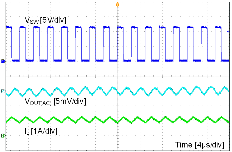
| VOUT = 5 V | IOUT = 1 A | fSW = 400 kHz |
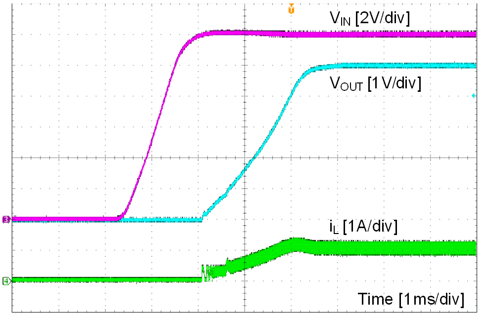
| VIN = 12 V | VOUT = 5 V | IOUT = 1 A |
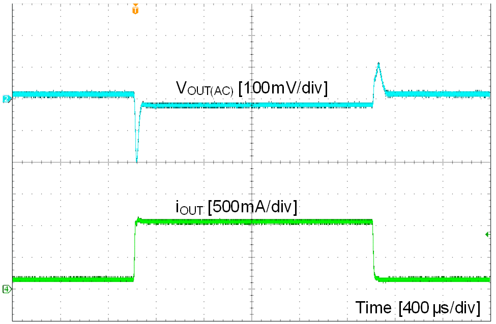
| VIN = 12 V | VOUT = 5 V | IOUT = 0.1 A to 1 A, 100 mA / μs |
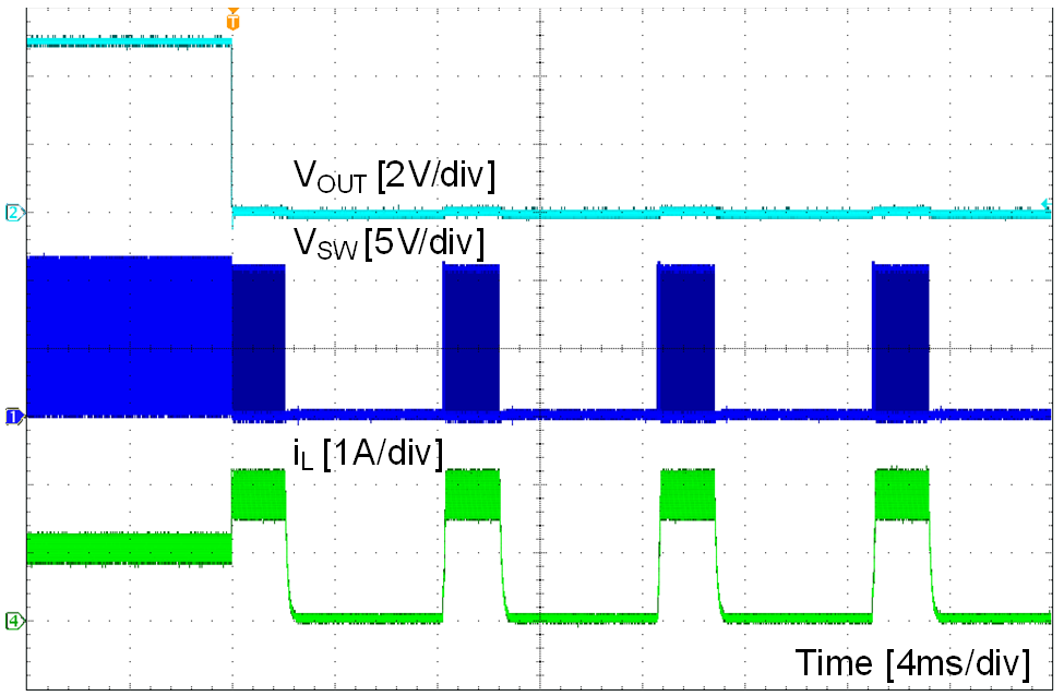
| VOUT = 5 V | IOUT = 1 A to short |
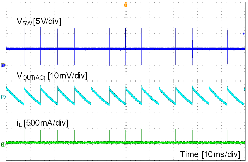
| VOUT = 5 V | IOUT = 0 mA | fSW = 400 kHz |
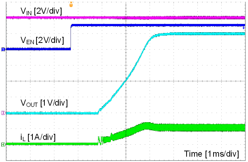
| VIN = 12 V | VOUT = 5 V | IOUT = 1 A |
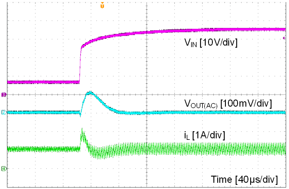
| VOUT = 7 V to 36 V, 2 V / μs | VOUT = 5 V | IOUT = 1 A |
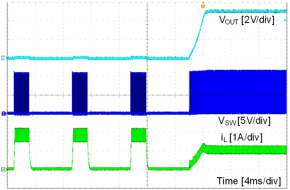
| VOUT = 5 V | IOUT = short to 1 A |