JAJSFN3C June 2018 – October 2020 LMR33630-Q1
PRODUCTION DATA
- 1 特長
- 2 アプリケーション
- 3 概要
- 4 Revision History
- 5 Pin Configuration and Functions
- 6 Specifications
- 7 Detailed Description
-
8 Application and Implementation
- 8.1 Application Information
- 8.2
Typical Application
- 8.2.1 Design Requirements
- 8.2.2
Detailed Design Procedure
- 8.2.2.1 Custom Design With WEBENCH® Tools
- 8.2.2.2 Choosing the Switching Frequency
- 8.2.2.3 Setting the Output Voltage
- 8.2.2.4 Inductor Selection
- 8.2.2.5 Output Capacitor Selection
- 8.2.2.6 Input Capacitor Selection
- 8.2.2.7 CBOOT
- 8.2.2.8 VCC
- 8.2.2.9 CFF Selection
- 8.2.2.10 External UVLO
- 8.2.2.11 Maximum Ambient Temperature
- 8.2.3 Application Curves
- 8.3 What to Do and What Not to Do
- 9 Power Supply Recommendations
- 10Layout
- 11Device and Documentation Support
パッケージ・オプション
デバイスごとのパッケージ図は、PDF版データシートをご参照ください。
メカニカル・データ(パッケージ|ピン)
- RNX|12
サーマルパッド・メカニカル・データ
- RNX|12
発注情報
7.3.2 Enable and Start-up
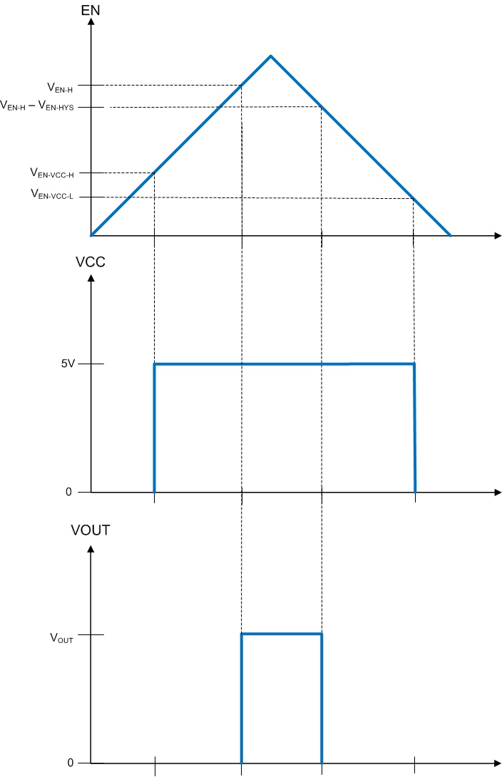
Start-up and shutdown are controlled by the EN input. This input features precision thresholds, allowing the use of an external voltage divider to provide an adjustable input UVLO (see Section 8.2.2.10). Applying a voltage of ≥ VEN-VCC_H causes the device to enter standby mode, powering the internal VCC, but not producing an output voltage. Increasing the EN voltage to VEN-H fully enables the device, allowing it to enter start-up mode and start the soft-start period. When the EN input is brought below VEN-H by VEN-HYS, the regulator stops running and enters standby mode. Further decrease in the EN voltage to below VEN-VCC-L completely shuts down the device. This behavior is shown in Figure 7-3. The EN input can be connected directly to VIN if this feature is not needed. This input must not be allowed to float. The values for the various EN thresholds can be found in Section 6.5.
The LMR33630-Q1 uses a reference-based soft start that prevents output voltage overshoots and large inrush currents as the regulator is starting up. A typical start-up waveform is shown in Figure 7-4, indicating typical timings. The rise time of the output voltage is about 4 ms (see the Section 6.5).
 Figure 7-3 Precision Enable Behavior
 Figure 7-4 Typical Start-up Behavior VIN = 12 V, VOUT = 5 V, IOUT = 3 A