JAJSIO6B September 2019 – September 2020 LMR36503-Q1
PRODUCTION DATA
- 1 特長
- 2 アプリケーション
- 3 概要
- 4 Revision History
- 5 Device Comparison Table
- 6 Pin Configuration and Functions
- 7 Specifications
-
8 Detailed Description
- 8.1 Overview
- 8.2 Functional Block Diagram
- 8.3
Feature Description
- 8.3.1 Enable, Start-up and Shutdown
- 8.3.2 External CLK SYNC (with MODE/SYNC)
- 8.3.3 Adjustable Switching Frequency (with RT)
- 8.3.4 Power-Good Output Operation
- 8.3.5 Internal LDO, VCC UVLO, and VOUT/BIAS Input
- 8.3.6 Bootstrap Voltage and VCBOOT-UVLO (CBOOT Terminal)
- 8.3.7 Output Voltage Selection
- 8.3.8 Soft Start and Recovery from Dropout
- 8.3.9 Current Limit and Short Circuit
- 8.3.10 Thermal Shutdown
- 8.3.11 Input Supply Current
- 8.4 Device Functional Modes
-
9 Application and Implementation
- 9.1 Application Information
- 9.2
Typical Application
- 9.2.1 Design Requirements
- 9.2.2 Detailed Design Procedure
- 9.2.3 Application Curves
- 9.3 What to Do and What Not to Do
- 10Power Supply Recommendations
- 11Layout
- 12Device and Documentation Support
- 13Mechanical, Packaging, and Orderable Information
パッケージ・オプション
メカニカル・データ(パッケージ|ピン)
- RPE|9
サーマルパッド・メカニカル・データ
- RPE|9
発注情報
9.2.2.2.1 FB for Adjustable Output
In an adjustable output voltage version, pin 8 of the device is FB. The output voltage of LMR36503-Q1 is externally adjustable using an external resistor divider network. The divider network is comprised of RFBT and RFBB, and closes the loop between the output voltage and the converter. The converter regulates the output voltage by holding the voltage on the FB pin equal to the internal reference voltage, VREF. The resistance of the divider is a compromise between excessive noise pickup and excessive loading of the output. Smaller values of resistance reduce noise sensitivity but also reduce the light-load efficiency. The recommended value for RFBT is 100 kΩ with a maximum value of 1 MΩ. Once RFBT is selected, Equation 6 is used to select RFBB. VREF is nominally 1 V. See Section 7.5.
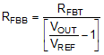
For this 5-V example, RFBT = 100 kΩ and RFBB = 24.9 kΩ is chosen.