JAJSIO6B September 2019 – September 2020 LMR36503-Q1
PRODUCTION DATA
- 1 特長
- 2 アプリケーション
- 3 概要
- 4 Revision History
- 5 Device Comparison Table
- 6 Pin Configuration and Functions
- 7 Specifications
-
8 Detailed Description
- 8.1 Overview
- 8.2 Functional Block Diagram
- 8.3
Feature Description
- 8.3.1 Enable, Start-up and Shutdown
- 8.3.2 External CLK SYNC (with MODE/SYNC)
- 8.3.3 Adjustable Switching Frequency (with RT)
- 8.3.4 Power-Good Output Operation
- 8.3.5 Internal LDO, VCC UVLO, and VOUT/BIAS Input
- 8.3.6 Bootstrap Voltage and VCBOOT-UVLO (CBOOT Terminal)
- 8.3.7 Output Voltage Selection
- 8.3.8 Soft Start and Recovery from Dropout
- 8.3.9 Current Limit and Short Circuit
- 8.3.10 Thermal Shutdown
- 8.3.11 Input Supply Current
- 8.4 Device Functional Modes
-
9 Application and Implementation
- 9.1 Application Information
- 9.2
Typical Application
- 9.2.1 Design Requirements
- 9.2.2 Detailed Design Procedure
- 9.2.3 Application Curves
- 9.3 What to Do and What Not to Do
- 10Power Supply Recommendations
- 11Layout
- 12Device and Documentation Support
- 13Mechanical, Packaging, and Orderable Information
パッケージ・オプション
メカニカル・データ(パッケージ|ピン)
- RPE|9
サーマルパッド・メカニカル・データ
- RPE|9
発注情報
8.3.3 Adjustable Switching Frequency (with RT)
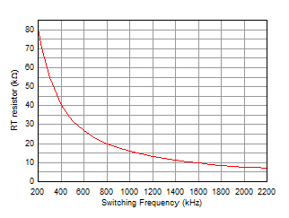
The select variants in the LMR36503-Q1 family with the RT pin allow the power designers to set any desired operating frequency between 200 kHz and 2.2 MHz in their applications. See Figure 8-7 to determine the resistor value needed for the desired switching frequency. The RT pin and the MODE/SYNC pin variants share the same pin location. The power supply designer can either use the RT pin variant and adjust the switching frequency of operation as warranted by the application or use the MODE/SYNC variant and synchronize to an external clock signal. See Table 8-2 for selection on programming the RT pin.
| RT INPUT | SWITCHING FREQUENCY |
|---|---|
| VCC | 1 MHz |
| GND | 2.2 MHz |
| RT to GND | Adjustable according to Figure 8-7 |
| Float (Not Recommended) | No Switching |
Equation 1 can be used to calculate the value of RT for a desired frequency.

where
- RT = Frequency setting resistor value (kΩ)
- FSW = Switching frequency (kHz)
 Figure 8-7 RT Values vs Frequency