JAJSIO6B September   2019  – September 2020 LMR36503-Q1

PRODUCTION DATA  

  1. 特長
  2. アプリケーション
  3. 概要
  4. Revision History
  5. Device Comparison Table
  6. Pin Configuration and Functions
    1.     Pin Functions
  7. Specifications
    1. 7.1 Absolute Maximum Ratings
    2. 7.2 ESD (Automotive) Ratings
    3. 7.3 Recommended Operating Conditions
    4. 7.4 Thermal Information
    5. 7.5 Electrical Characteristics
    6. 7.6 Timing Characteristics
    7. 7.7 Switching Characteristics
    8. 7.8 System Characteristics
    9. 7.9 Typical Characteristics
  8. Detailed Description
    1. 8.1 Overview
    2. 8.2 Functional Block Diagram
    3. 8.3 Feature Description
      1. 8.3.1  Enable, Start-up and Shutdown
      2. 8.3.2  External CLK SYNC (with MODE/SYNC)
        1. 8.3.2.1 Pulse-Dependent MODE/SYNC Pin Control
      3. 8.3.3  Adjustable Switching Frequency (with RT)
      4. 8.3.4  Power-Good Output Operation
      5. 8.3.5  Internal LDO, VCC UVLO, and VOUT/BIAS Input
      6. 8.3.6  Bootstrap Voltage and VCBOOT-UVLO (CBOOT Terminal)
      7. 8.3.7  Output Voltage Selection
      8. 8.3.8  Soft Start and Recovery from Dropout
        1. 8.3.8.1 Recovery from Dropout
      9. 8.3.9  Current Limit and Short Circuit
      10. 8.3.10 Thermal Shutdown
      11. 8.3.11 Input Supply Current
    4. 8.4 Device Functional Modes
      1. 8.4.1 Shutdown Mode
      2. 8.4.2 Standby Mode
      3. 8.4.3 Active Mode
        1. 8.4.3.1 CCM Mode
        2. 8.4.3.2 Auto Mode - Light Load Operation
          1. 8.4.3.2.1 Diode Emulation
          2. 8.4.3.2.2 Frequency Reduction
        3. 8.4.3.3 FPWM Mode - Light Load Operation
        4. 8.4.3.4 Minimum On-time (High Input Voltage) Operation
        5. 8.4.3.5 Dropout
  9. Application and Implementation
    1. 9.1 Application Information
    2. 9.2 Typical Application
      1. 9.2.1 Design Requirements
      2. 9.2.2 Detailed Design Procedure
        1. 9.2.2.1 Choosing the Switching Frequency
        2. 9.2.2.2 Setting the Output Voltage
          1. 9.2.2.2.1 FB for Adjustable Output
        3. 9.2.2.3 Inductor Selection
        4. 9.2.2.4 Output Capacitor Selection
        5. 9.2.2.5 Input Capacitor Selection
        6. 9.2.2.6 CBOOT
        7. 9.2.2.7 VCC
        8. 9.2.2.8 CFF Selection
          1. 9.2.2.8.1 External UVLO
        9. 9.2.2.9 Maximum Ambient Temperature
      3. 9.2.3 Application Curves
    3. 9.3 What to Do and What Not to Do
  10. 10Power Supply Recommendations
  11. 11Layout
    1. 11.1 Layout Guidelines
      1. 11.1.1 Ground and Thermal Considerations
    2. 11.2 Layout Example
  12. 12Device and Documentation Support
    1. 12.1 Documentation Support
      1. 12.1.1 Related Documentation
    2. 12.2 ドキュメントの更新通知を受け取る方法
    3. 12.3 サポート・リソース
    4. 12.4 Trademarks
    5. 12.5 静電気放電に関する注意事項
    6. 12.6 用語集
  13. 13Mechanical, Packaging, and Orderable Information

パッケージ・オプション

メカニカル・データ(パッケージ|ピン)
サーマルパッド・メカニカル・データ
発注情報

Typical Characteristics

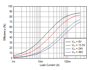
Unless otherwise specified, the following conditions apply: TA = 25°C, VIN = 13.5 V.
GUID-20200813-CA0I-VSFR-JSNG-3B41NZG64MSB-low.gif
VOUT = 3.3 V Fixed FSW = 2.2 MHz (FPWM)
Figure 7-1 Efficiency 3.3-V Output, FPWM
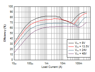
GUID-20200813-CA0I-22HG-ZPFR-2STGCFWFNTKR-low.gif
VOUT = 5 V Fixed FSW-NOM = 2.2 MHz (Auto)
Figure 7-3 Efficiency 5-V Output, Auto Mode
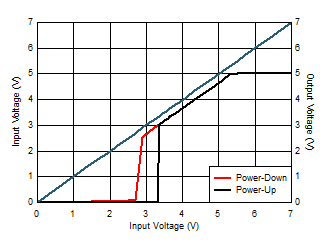
GUID-DDF11E60-9628-4DA0-853A-B573A60767B7-low.gif
ILoad = 300 mA VOUT = 5 V Fixed FSW-NOM = 2.2 MHz (Auto)
Figure 7-5 Dropout at Power-Up and Power-Down
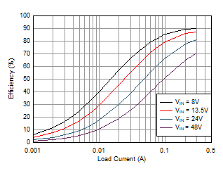
GUID-20200813-CA0I-4D0N-DXHD-CG1VGH0F007B-low.gif
VOUT = 5 V Fixed FSW = 2.2 MHz (FPWM)
Figure 7-2 Efficiency 5-V Output, FPWM
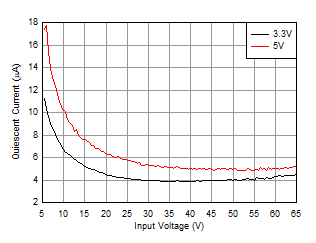
GUID-20200906-CA0I-P5VL-K6DK-D66BW3M3RS4V-low.gifFigure 7-4 Typical Input Supply Current at No Load for Fixed 3.3-V and 5-V Output
GUID-3561D989-3927-41C2-95FF-FF1BCD912270-low.gif
 
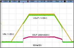
Figure 7-6 Typical Start-up and Shutdown at VOUT = 5 V