JAJSJR5A October   2019  – November 2020 LMR50410-Q1

PRODUCTION DATA  

  1. 特長
  2. アプリケーション
  3. 説明
  4. Revision History
  5. Device Comparison Table
  6. Pin Configuration and Functions
  7. Specifications
    1. 7.1 Absolute Maximum Ratings
    2. 7.2 ESD Ratings
    3. 7.3 Recommended Operating Conditions
    4. 7.4 Thermal Information
    5. 7.5 Electrical Characteristics
    6. 7.6 Timing Requirements
    7. 7.7 Switching Characteristics
    8. 7.8 System Characteristics
    9. 7.9 Typical Characteristics
  8. Detailed Description
    1. 8.1 Overview
    2. 8.2 Functional Block Diagram
    3. 8.3 Feature Description
      1. 8.3.1 Fixed Frequency Peak Current Mode Control
      2. 8.3.2 Adjustable Output Voltage
      3. 8.3.3 Enable
      4. 8.3.4 Minimum ON-Time, Minimum OFF-Time, and Frequency Foldback
      5. 8.3.5 Bootstrap Voltage
      6. 8.3.6 Overcurrent and Short Circuit Protection
      7. 8.3.7 Soft Start
      8. 8.3.8 Thermal Shutdown
    4. 8.4 Device Functional Modes
      1. 8.4.1 Shutdown Mode
      2. 8.4.2 Active Mode
      3. 8.4.3 CCM Mode
      4. 8.4.4 Light-Load Operation (PFM Version)
      5. 8.4.5 Light-Load Operation (FPWM Version)
  9. Application and Implementation
    1. 9.1 Application Information
    2. 9.2 Typical Application
      1. 9.2.1 Design Requirements
      2. 9.2.2 Detailed Design Procedure
        1. 9.2.2.1 Custom Design With WEBENCH® Tools
        2. 9.2.2.2 Output Voltage Set-Point
        3. 9.2.2.3 Switching Frequency
        4. 9.2.2.4 Inductor Selection
        5. 9.2.2.5 Output Capacitor Selection
        6. 9.2.2.6 Input Capacitor Selection
        7. 9.2.2.7 Bootstrap Capacitor
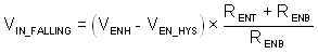
        8. 9.2.2.8 Undervoltage Lockout Set-Point
        9. 9.2.2.9 Maximum Ambient Temperature
      3. 9.2.3 Application Curves
  10. 10Power Supply Recommendations
  11. 11Layout
    1. 11.1 Layout Guidelines
      1. 11.1.1 Compact Layout for EMI Reduction
      2. 11.1.2 Feedback Resistors
    2. 11.2 Layout Example
  12. 12Device and Documentation Support
    1. 12.1 Device Support
      1. 12.1.1 Development Support
        1. 12.1.1.1 Custom Design With WEBENCH® Tools
    2. 12.2 Documentation Support
      1. 12.2.1 Related Documentation
    3. 12.3 ドキュメントの更新通知を受け取る方法
    4. 12.4 サポート・リソース
    5. 12.5 Trademarks
    6. 12.6 静電気放電に関する注意事項
    7. 12.7 用語集
  13. 13Mechanical, Packaging, and Orderable Information

パッケージ・オプション

メカニカル・データ(パッケージ|ピン)
サーマルパッド・メカニカル・データ
発注情報

Undervoltage Lockout Set-Point

The system undervoltage lockout (UVLO) is adjusted using the external voltage divider network of RENT and RENB. The UVLO has two thresholds, one for power up when the input voltage is rising and one for power down or brown outs when the input voltage is falling. Equation 13 can be used to determine the VIN UVLO level.

Equation 13. GUID-B8E07E41-11C0-4D13-9774-8E60417B9154-low.gif

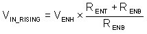
The EN rising threshold (VENH) for LMR50410-Q1 is set to be 1.23 V (typical). Choose a value of 200 kΩ for RENB to minimize input current from the supply. If the desired VIN UVLO level is at 6.0 V, then the value of RENT can be calculated using Equation 14:

Equation 14. GUID-3BF17590-1703-4B8E-B7CF-5D159377AC77-low.gif

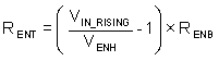
The above equation yields a value of 775.6 kΩ, a standard value of 768 kΩ is selected. The resulting falling UVLO threshold, equals 5.3 V, can be calculated by Equation 15 where EN hysteresis voltage, VEN_HYS, is 0.13 V (typical).

Equation 15. GUID-2F7E1299-891B-4220-B78B-02E84D790644-low.gif