JAJSJR5A October 2019 – November 2020 LMR50410-Q1
PRODUCTION DATA
- 1 特長
- 2 アプリケーション
- 3 説明
- 4 Revision History
- 5 Device Comparison Table
- 6 Pin Configuration and Functions
- 7 Specifications
- 8 Detailed Description
-
9 Application and Implementation
- 9.1 Application Information
- 9.2
Typical Application
- 9.2.1 Design Requirements
- 9.2.2
Detailed Design Procedure
- 9.2.2.1 Custom Design With WEBENCH® Tools
- 9.2.2.2 Output Voltage Set-Point
- 9.2.2.3 Switching Frequency
- 9.2.2.4 Inductor Selection
- 9.2.2.5 Output Capacitor Selection
- 9.2.2.6 Input Capacitor Selection
- 9.2.2.7 Bootstrap Capacitor
- 9.2.2.8 Undervoltage Lockout Set-Point
- 9.2.2.9 Maximum Ambient Temperature
- 9.2.3 Application Curves
- 10Power Supply Recommendations
- 11Layout
- 12Device and Documentation Support
- 13Mechanical, Packaging, and Orderable Information
9.2 Typical Application
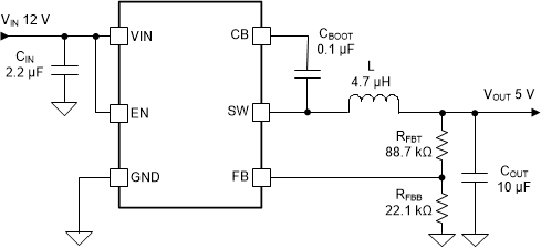
The LMR50410-Q1 only requires a few external components to convert from a wide voltage range supply to a fixed output voltage. Figure 9-1 shows a basic schematic.
 Figure 9-1 Application Circuit
The external components have to fulfill the needs of the application and the stability criteria of the control loop of the device. Table 9-1 can be used to simplify the output filter component selection.
Table 9-1 L and COUT Typical Values
| fSW (MHz) | VOUT (V) | L (µH) | COUT (µF) (1) | RFBT (kΩ) | RFBB (kΩ) |
|---|---|---|---|---|---|
| 2.1 | 3.3 | 3.3 | 10 µF / 10 V | 51 | 22.1 |
| 5 | 4.7 | 10 µF / 10 V | 88.7 | 22.1 | |
| 12 | 10 | 22 µF / 25 V | 243 | 22.1 |
(1) Ceramic capacitor is used in this
table.