JAJSV98 August 2024 LMR51460-Q1
PRODUCTION DATA
- 1
- 1 特長
- 2 アプリケーション
- 3 概要
- 4 Device Comparison Table
- 5 Pin Configuration and Functions
- 6 Specifications
-
7 Detailed Description
- 7.1 Overview
- 7.2 Functional Block Diagram
- 7.3
Feature Description
- 7.3.1 Fixed Frequency Peak Current Mode Control
- 7.3.2 Adjustable Output Voltage
- 7.3.3 Enable
- 7.3.4 Switching Frequency
- 7.3.5 Power-Good Flag Output
- 7.3.6 Minimum ON-Time, Minimum OFF-Time, and Frequency Foldback
- 7.3.7 Bootstrap Voltage
- 7.3.8 Overcurrent and Short-Circuit Protection
- 7.3.9 Soft Start
- 7.3.10 Thermal Shutdown
- 7.4 Device Functional Modes
- 8 Application and Implementation
- 9 Device and Documentation Support
- 10Revision History
- 11Mechanical, Packaging, and Orderable Information
7.3.1 Fixed Frequency Peak Current Mode Control
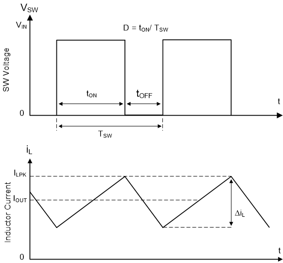
The following operating description of the LMR51460-Q1 refers to Functional Block Diagram and to the waveforms in Figure 7-1. The LMR51460-Q1 is a step-down synchronous buck converter with integrated high-side (HS) and low-side (LS) switches (synchronous rectifier). The LMR51460-Q1 supplies a regulated output voltage by turning on the high-side and low-side NMOS switches with controlled duty cycle. During high-side switch ON time, the SW pin voltage swings up to approximately VIN, and the inductor current, iL, increases with linear slope (VIN – VOUT) / L. When the high-side switch is turned off by the control logic, the low-side switch is turned on after an anti-shoot-through dead time. Inductor current discharges through the low-side switch with a slope of –VOUT / L. The control parameter of a buck converter is defined as Duty Cycle D = tON / TSW, where tON is the high-side switch ON time and TSW is the switching period. The converter control loop maintains a constant output voltage by adjusting the duty cycle D. In an ideal buck converter, where losses are ignored, D is proportional to the output voltage and inversely proportional to the input voltage: D = VOUT / VIN.
 Figure 7-1 SW Node and Inductor Current Waveforms in Continuous Conduction Mode (CCM)
The LMR51460-Q1 employs fixed-frequency peak-current mode control. A voltage feedback loop is used to get accurate DC voltage regulation by adjusting the peak-current command based on voltage offset. The peak inductor current is sensed from the high-side switch and compared to the peak current threshold to control the ON time of the high-side switch. The voltage feedback loop is internally-compensated, which allows for fewer external components, making designing easy, and providing stable operation when using a variety of output capacitors. The converter operates with fixed switching frequency at normal load conditions. During light-load condition, the LMR51460-Q1 operates in PFM mode to maintain high efficiency (PFM version) or in FPWM mode for low output voltage ripple, tight output voltage regulation, and constant switching frequency (FPWM version).