JAJSV98 August 2024 LMR51460-Q1
PRODUCTION DATA
- 1
- 1 特長
- 2 アプリケーション
- 3 概要
- 4 Device Comparison Table
- 5 Pin Configuration and Functions
- 6 Specifications
-
7 Detailed Description
- 7.1 Overview
- 7.2 Functional Block Diagram
- 7.3
Feature Description
- 7.3.1 Fixed Frequency Peak Current Mode Control
- 7.3.2 Adjustable Output Voltage
- 7.3.3 Enable
- 7.3.4 Switching Frequency
- 7.3.5 Power-Good Flag Output
- 7.3.6 Minimum ON-Time, Minimum OFF-Time, and Frequency Foldback
- 7.3.7 Bootstrap Voltage
- 7.3.8 Overcurrent and Short-Circuit Protection
- 7.3.9 Soft Start
- 7.3.10 Thermal Shutdown
- 7.4 Device Functional Modes
- 8 Application and Implementation
- 9 Device and Documentation Support
- 10Revision History
- 11Mechanical, Packaging, and Orderable Information
7.3.3 Enable
The voltage on the EN pin controls the ON and OFF operation of the LMR51460-Q1. A voltage of less than 0.8V shuts down the device, while a voltage of greater than 1.4V is required to start the converter. The EN pin is an input and cannot be left open or floating. The simplest way to enable the operation of the LMR51460-Q1 when VIN is within the operating range.
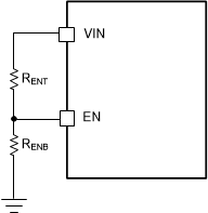
Many applications benefit from the employment of an enable divider RENT and RENB (Figure 7-3) to establish a precision system UVLO level for the converter. System UVLO can be used for supplies operating from utility power as well as battery power. System UVLO can be used for sequencing, making sure of reliable operation or supplying protection, such as a battery discharge level. An external logic signal can also be used to drive EN input for system sequencing and protection. Note, the EN pin voltage must not to be greater than VIN + 0.3V. TI does not recommend to apply EN voltage when VIN is 0V.
 Figure 7-3 System UVLO by Enable Divider