JAJSR66 September   2024 LMR66430-EP

PRODUCTION DATA  

  1.   1
  2. 特長
  3. アプリケーション
  4. 概要
  5. Device Comparison Table
  6. Pin Configuration and Functions
  7. Specifications
    1. 6.1 Absolute Maximum Ratings
    2. 6.2 ESD Ratings
    3. 6.3 Recommended Operating Conditions
    4. 6.4 Thermal Information
    5. 6.5 Electrical Characteristics
    6. 6.6 Typical Characteristics
  8. Detailed Description
    1. 7.1 Overview
    2. 7.2 Functional Block Diagram
    3. 7.3 Feature Description
      1. 7.3.1  Enable, Start-Up, and Shutdown
      2. 7.3.2  External CLK SYNC (with MODE/SYNC)
        1. 7.3.2.1 Pulse-Dependent MODE/SYNC Pin Control
      3. 7.3.3  Adjustable Switching Frequency (with RT)
      4. 7.3.4  Power-Good Output Operation
      5. 7.3.5  Internal LDO, VCC, and VOUT/FB Input
      6. 7.3.6  Bootstrap Voltage and VBOOT-UVLO (BOOT Terminal)
      7. 7.3.7  Output Voltage Selection
      8. 7.3.8  Spread Spectrum
      9. 7.3.9  Soft Start and Recovery from Dropout
        1. 7.3.9.1 Recovery from Dropout
      10. 7.3.10 Current Limit and Short Circuit
      11. 7.3.11 Thermal Shutdown
      12. 7.3.12 Input Supply Current
    4. 7.4 Device Functional Modes
      1. 7.4.1 Shutdown Mode
      2. 7.4.2 Standby Mode
      3. 7.4.3 Active Mode
        1. 7.4.3.1 CCM Mode
        2. 7.4.3.2 Auto Mode – Light Load Operation
          1. 7.4.3.2.1 Diode Emulation
          2. 7.4.3.2.2 Frequency Reduction
        3. 7.4.3.3 FPWM Mode – Light Load Operation
        4. 7.4.3.4 Minimum On-Time (High Input Voltage) Operation
        5. 7.4.3.5 Dropout
  9. Application and Implementation
    1. 8.1 Application Information
    2. 8.2 Typical Application
      1. 8.2.1 LMR66430-EP Design Guide
      2. 8.2.2 Design Requirements
      3. 8.2.3 Detailed Design Procedure
        1. 8.2.3.1  Choosing the Switching Frequency
        2. 8.2.3.2  Setting the Output Voltage
        3. 8.2.3.3  Inductor Selection
        4. 8.2.3.4  Output Capacitor Selection
        5. 8.2.3.5  Input Capacitor Selection
        6. 8.2.3.6  CBOOT
        7. 8.2.3.7  VCC
        8. 8.2.3.8  CFF Selection
        9. 8.2.3.9  External UVLO
        10. 8.2.3.10 Maximum Ambient Temperature
      4. 8.2.4 Application Curves
    3. 8.3 Best Design Practices
    4. 8.4 Power Supply Recommendations
    5. 8.5 Layout
      1. 8.5.1 Layout Guidelines
        1. 8.5.1.1 Ground and Thermal Considerations
      2. 8.5.2 Layout Example
  10. Device and Documentation Support
    1. 9.1 Device Support
      1. 9.1.1 サード・パーティ製品に関する免責事項
      2. 9.1.2 Device Nomenclature
    2. 9.2 Documentation Support
      1. 9.2.1 Related Documentation
    3. 9.3 ドキュメントの更新通知を受け取る方法
    4. 9.4 サポート・リソース
    5. 9.5 Trademarks
    6. 9.6 静電気放電に関する注意事項
    7. 9.7 用語集
  11. 10Revision History
  12. 11Mechanical, Packaging, and Orderable Information
    1. 11.1 Tape and Reel Information

パッケージ・オプション

メカニカル・データ(パッケージ|ピン)
サーマルパッド・メカニカル・データ
発注情報

Application Curves

LMR66430-EP LMR66430MB3RBXNEP Efficiency (Mode = Auto)Figure 8-4 LMR66430MB3RBXNEP Efficiency (Mode = Auto)
LMR66430-EP LMR66430MB3RBXNEP Efficiency (Mode = FPWM)Figure 8-6 LMR66430MB3RBXNEP Efficiency (Mode = FPWM)
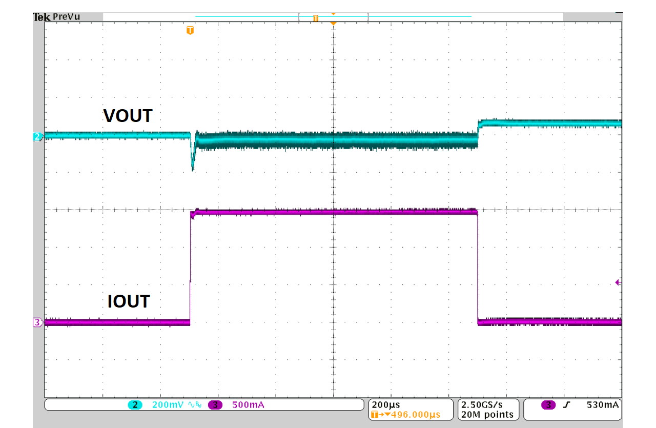
LMR66430-EP Load
            Transient
LMR66430MB3RBXNEP VOUT = 3.3V (Fix)
0A to 1.5A,1A/µs Mode = auto
Figure 8-8 Load Transient
LMR66430-EP Output Voltage Ripple
LMR66430MB3RBXNEP 3A load
Figure 8-10 Output Voltage Ripple
LMR66430-EP LMR66430-2EVM Thermal
            Performance
IC Inductor Ambient Temperature
LMR66430MB3RBXNEP XGL5030-472 22°C
Figure 8-12 LMR66430-2EVM Thermal Performance
LMR66430-EP LMR66430MB3RBXNEP Power Dissipation
            (Mode = Auto)Figure 8-5 LMR66430MB3RBXNEP Power Dissipation (Mode = Auto)
LMR66430-EP LMR66430MB3RBXNEP Power Dissipation (Mode = FPWM)Figure 8-7 LMR66430MB3RBXNEP Power Dissipation (Mode = FPWM)
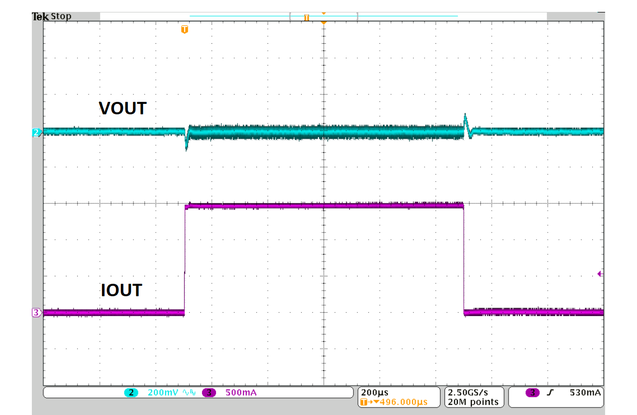
LMR66430-EP Load
            Transient
LMR66430MB3RBXNEP VOUT = 3.3V (Fix)
0A to 1.5A,1A/µs Mode = FPWM
Figure 8-9 Load Transient
LMR66430-EP Output Voltage Ripple
LMR66430MB3RBXNEP 0A load
Figure 8-11 Output Voltage Ripple
LMR66430-EP CISPR 11/32, Class B, Conducted EMI
VIN = 12V VOUT = 3.3V Fsw = 1MHz
Load = 3A LMR66430-2EVM FB1=5.6μH, C5 = 4.7μF
Figure 8-13 CISPR 11/32, Class B, Conducted EMI