JAJSR66 September 2024 LMR66430-EP
PRODUCTION DATA
- 1
- 1 特長
- 2 アプリケーション
- 3 概要
- 4 Device Comparison Table
- 5 Pin Configuration and Functions
- 6 Specifications
-
7 Detailed Description
- 7.1 Overview
- 7.2 Functional Block Diagram
- 7.3
Feature Description
- 7.3.1 Enable, Start-Up, and Shutdown
- 7.3.2 External CLK SYNC (with MODE/SYNC)
- 7.3.3 Adjustable Switching Frequency (with RT)
- 7.3.4 Power-Good Output Operation
- 7.3.5 Internal LDO, VCC, and VOUT/FB Input
- 7.3.6 Bootstrap Voltage and VBOOT-UVLO (BOOT Terminal)
- 7.3.7 Output Voltage Selection
- 7.3.8 Spread Spectrum
- 7.3.9 Soft Start and Recovery from Dropout
- 7.3.10 Current Limit and Short Circuit
- 7.3.11 Thermal Shutdown
- 7.3.12 Input Supply Current
- 7.4 Device Functional Modes
- 8 Application and Implementation
- 9 Device and Documentation Support
- 10Revision History
- 11Mechanical, Packaging, and Orderable Information
7.3.7 Output Voltage Selection
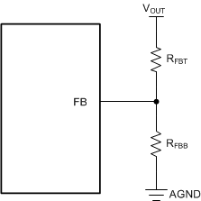
In the device family, an adjustable output or fixed output voltage option is configurable for every device variant (see Section 4). For an adjustable output, the user needs an external resistor divider connection between the output voltage node, the device FB pin, and the system GND, as shown in Figure 7-9. The adjustable output voltage operation uses a 1V internal reference voltage.
When using the fixed-output configuration from the device family, simply connect the FB pin (identified as VOUT/FB pin for fixed-output variants in the rest of the data sheet) to the system output voltage node. See Section 4 for more details.
 Figure 7-9 Setting Output Voltage for Adjustable Output Variant
In adjustable output voltage configuration, an additional feedforward capacitor, CFF, in parallel with the RFBT, can be used to optimize the phase margin and transient response. See Section 8.2.3.8 for more details. No additional resistor divider or feedforward capacitor is needed in fixed-output variants.
Programming the output voltage can be achieved by selecting the top feedback resistance, RFBT (that is, 100kΩ), then calculating for RFBB (Equation 2). The additional criteria is that the minimum value for the parallel combination of RFBT and RFBB is greater than 5kΩ (Equation 3).