JAJSDW2C November   2016  – August 2021 LMS3635-Q1 , LMS3655-Q1

PRODUCTION DATA  

  1. 特長
  2. アプリケーション
  3. 概要
  4. Revision History
  5. Device Comparison Tables
  6. Pin Configuration and Functions
  7. Specifications
    1. 7.1 Absolute Maximum Ratings
    2. 7.2 ESD Ratings
    3. 7.3 Recommended Operating Conditions
    4. 7.4 Thermal Information
    5. 7.5 Thermal Information (for Device Mounted on PCB)
    6. 7.6 Electrical Characteristics
    7. 7.7 System Characteristics
    8. 7.8 Timing Requirements
    9. 7.9 Typical Characteristics
  8. Detailed Description
    1. 8.1 Overview
    2. 8.2 Functional Block Diagram
      1. 8.2.1 Control Scheme
    3. 8.3 Feature Description
      1. 8.3.1 RESET Flag Output
      2. 8.3.2 Enable and Start-Up
      3. 8.3.3 Soft-Start Function
      4. 8.3.4 Current Limit
      5. 8.3.5 Hiccup Mode
      6. 8.3.6 Synchronizing Input
      7. 8.3.7 Undervoltage Lockout (UVLO) and Thermal Shutdown (TSD)
      8. 8.3.8 Input Supply Current
    4. 8.4 Device Functional Modes
      1. 8.4.1 AUTO Mode
      2. 8.4.2 FPWM Mode
      3. 8.4.3 Dropout
      4. 8.4.4 Spread-Spectrum Operation
  9. Application and Implementation
    1. 9.1 Application Information
    2. 9.2 Typical Applications
      1. 9.2.1 General Application
        1. 9.2.1.1 Design Requirements
        2. 9.2.1.2 Detailed Design Procedure
          1. 9.2.1.2.1 Custom Design With WEBENCH® Tools
          2. 9.2.1.2.2 External Components Selection
            1. 9.2.1.2.2.1 Input Capacitors
            2. 9.2.1.2.2.2 Output Inductors and Capacitors
              1. 9.2.1.2.2.2.1 Inductor Selection
              2. 9.2.1.2.2.2.2 Output Capacitor Selection
          3. 9.2.1.2.3 Setting the Output Voltage
          4. 9.2.1.2.4 FB for Adjustable Output
          5. 9.2.1.2.5 VCC
          6. 9.2.1.2.6 BIAS
          7. 9.2.1.2.7 CBOOT
          8. 9.2.1.2.8 Maximum Ambient Temperature
        3. 9.2.1.3 Application Curves
      2. 9.2.2 Fixed 5-V Output for USB-Type Applications
        1. 9.2.2.1 Design Requirements
        2. 9.2.2.2 Detailed Design Procedure
        3. 9.2.2.3 Application Curves
      3. 9.2.3 Fixed 3.3-V Output
        1. 9.2.3.1 Design Requirements
        2. 9.2.3.2 Detailed Design Procedure
        3. 9.2.3.3 Application Curves
      4. 9.2.4 6-V Adjustable Output
        1. 9.2.4.1 Design Requirements
        2. 9.2.4.2 Detailed Design Procedure
        3. 9.2.4.3 Application Curves
    3. 9.3 Do's and Don't's
  10. 10Power Supply Recommendations
  11. 11Layout
    1. 11.1 Layout Guidelines
    2. 11.2 Layout Example
  12. 12Device and Documentation Support
    1. 12.1 Device Support
      1. 12.1.1 Third-Party Products Disclaimer
      2. 12.1.2 Development Support
        1. 12.1.2.1 Custom Design With WEBENCH® Tools
    2. 12.2 Documentation Support
      1. 12.2.1 Related Documentation
    3. 12.3 Receiving Notification of Documentation Updates
    4. 12.4 サポート・リソース
    5. 12.5 Trademarks
    6. 12.6 Electrostatic Discharge Caution
    7. 12.7 Glossary
  13. 13Mechanical, Packaging, and Orderable Information

パッケージ・オプション

メカニカル・データ(パッケージ|ピン)
サーマルパッド・メカニカル・データ
発注情報

Application Curves

The following characteristics apply only to the circuit of Figure 9-16. These parameters are not tested and represent typical performance only. Unless otherwise stated, the following conditions apply: VIN = 12 V, TA = 25°C. For the purpose of offering more information to the designer, information for the application with FPWM pin high (FPWM mode) and FPWM pin low (AUTO mode) is included, although the schematic shows the application running specifically in AUTO mode. The mode is specified under each of the following graphs.

GUID-E26A2C56-C9CC-40B9-A95B-26CCBF4B3C61-low.gif
VOUT = 3.3 V AUTO
Figure 9-17 Efficiency
GUID-A0621BDB-5AE2-4A03-ADC0-783AE577BAE2-low.gif
VOUT = 3.3 V AUTO
Figure 9-19 Load and Line Regulation
GUID-A25C70B4-BB9A-4AE1-882F-ED7B3EFD87CB-low.gif
VOUT = 3.3 V AUTO IOUT = 0 A
Figure 9-21 Input Supply Current (Includes Leakage Current of Capacitor)
GUID-082D8029-897D-411F-AA9B-D305D0905811-low.gif
VOUT = 3.3 V
Figure 9-23 Dropout for –3% Regulation
GUID-5928B2A2-D85D-4E17-A95D-7AACAF01AFE8-low.gif
VOUT = 3.3 V AUTO
Figure 9-25 Switching Frequency vs Load Current
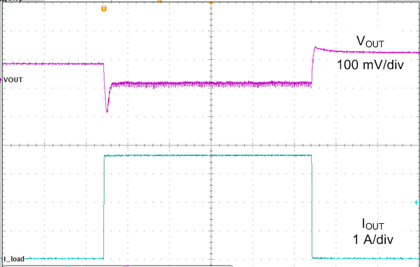
GUID-F6885C4E-B1B2-43F8-BD31-843E86920E40-low.png
AUTO VOUT = 3.3 V L = 10 µH,
COUT = 190 µF IOUT = 0 A to 3.5 A TR = TF = 1 µs
Figure 9-27 Load Transient
GUID-2D29F9DE-2596-4684-9E5E-55A05D1718E5-low.png
VOUT = 3.3 V IOUT = 10 mA
Figure 9-29 Mode Change Transient AUTO to FPWM mode
GUID-C83E3D4D-B952-4CF6-B0A2-523E73432753-low.gif
VOUT = 3.3 V FPWM
Figure 9-18 Efficiency
GUID-33D257C0-E18F-424F-A1AF-09541453D840-low.gif
VOUT = 3.3 V FPWM
Figure 9-20 Load and Line Regulation
GUID-C6647459-E49C-4106-82F9-EECA5F028BB4-low.gif
VOUT = 3.3 V
Figure 9-22 Load Current for PFM-to-PWM Transition
GUID-D236763F-1FEC-4AA7-BD96-839464685C56-low.gif
VOUT = 3.3 V
Figure 9-24 Dropout for ≥ 330 kHz
GUID-AC52BA80-F917-4BC7-A87A-34E322EBC1FE-low.gif
VOUT = 3.3 V L = 10 µH
Figure 9-26 Output Current Level for Overcurrent Protection Trip
GUID-933325B5-3032-455A-BA9F-FF40CF980D6B-low.png
FPWM VOUT = 3.3 V L = 10 µH,
COUT = 190 µF IOUT = 0 A to 3.5 A TR = TF = 1 µs
Figure 9-28 Load Transient