SNOSC70C April 2012 – July 2016 LMV601 , LMV602 , LMV604
PRODUCTION DATA.
- 1 Features
- 2 Applications
- 3 Description
- 4 Revision History
- 5 Pin Configuration and Functions
-
6 Specifications
- 6.1 Absolute Maximum Ratings
- 6.2 ESD Ratings
- 6.3 Recommended Operating Conditions
- 6.4 Thermal Information
- 6.5 Electrical Characteristics - DC (2.7 V)
- 6.6 Electrical Characteristics - AC (2.7 V)
- 6.7 Electrical Characteristics - DC (5 V)
- 6.8 Electrical Characteristics - AC (5 V)
- 6.9 Typical Characteristics
- 7 Detailed Description
- 8 Application and Implementation
- 9 Power Supply Recommendations
- 10Layout
- 11Device and Documentation Support
- 12Mechanical, Packaging, and Orderable Information
7 Detailed Description
7.1 Overview
The LMV60x family of amplifiers features low-voltage, low-power, and rail-to-rail output operational amplifiers designed for low-voltage portable applications. The family is designed using all CMOS technology. This results in an ultra-low input bias current. The LMV601 has a shutdown option, which can be used in portable devices to increase battery life.
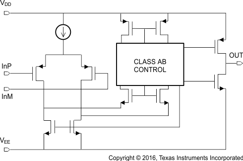
A simplified schematic of the LMV60x family of amplifiers is shown in Functional Block Diagram. The PMOS input differential pair allows the input to include ground. The output of this differential pair is connected to the Class AB turnaround stage. This Class AB turnaround has a lower quiescent current, compared to regular turnaround stages. This results in lower offset, noise, and power dissipation, while slew rate equals that of a conventional turnaround stage. The output of the Class AB turnaround stage provides gate voltage to the complementary common-source transistors at the output stage. These transistors enable the device to have rail-to-rail output.
7.2 Functional Block Diagram
7.3 Feature Description
7.3.1 Class AB Turnaround Stage Amplifier
This patented folded cascode stage has a combined class AB amplifier stage, which replaces the conventional folded cascode stage. Therefore, the class AB folded cascode stage runs at a much lower quiescent current compared to conventional folded cascode stages. This results in significantly smaller offset and noise contributions. The reduced offset and noise contributions in turn reduce the offset voltage level and the voltage noise level at the input of the LMV60x. Also the lower quiescent current results in a high open-loop gain for the amplifier. The lower quiescent current does not affect the slew rate of the amplifier nor its ability to handle the total current swing coming from the input stage.
The input voltage noise of the device at low frequencies, below 1 kHz, is slightly higher than devices with a BJT input stage. However, the PMOS input stage results in a much lower input bias current and the input voltage noise drops at frequencies above 1 kHz.
7.4 Device Functional Modes
7.4.1 Low Input Bias Current
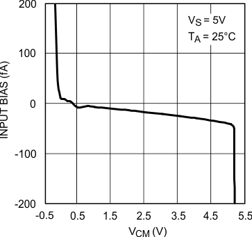
The LMV60x amplifiers have a PMOS input stage. As a result, they have a much lower input bias current than devices with BJT input stages. This feature makes these devices ideal for sensor circuits. A typical curve of the input bias current of the LMV601 is shown in Figure 41.
7.4.2 Shutdown Feature
The LMV601 is capable of being turned off to conserve power and increase battery life in portable devices. Once in shutdown mode the supply current is drastically reduced, 1 µA maximum, and the output is tri-stated.
The device is disabled when the shutdown pin voltage is pulled low. The shutdown pin must never be left unconnected. Leaving the pin floating results in an undefined operation mode and the device may oscillate between shutdown and active modes.
The LMV601 typically turns on 2.8 µs after the shutdown voltage is pulled high. The device turns off in less than 400 ns after shutdown voltage is pulled low. Figure 42 and Figure 43 show the turnon and turnoff time of the LMV601, respectively. To reduce the effect of the capacitance added to the circuit by the scope probe, in the turnoff time circuit a resistive load of 600 Ω is added. Figure 44 and Figure 45 show the test circuits used to obtain the two plots.
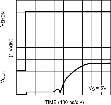 Figure 42. Turnon Time
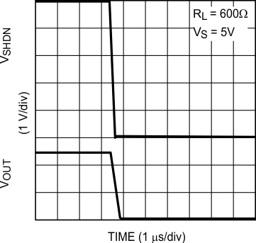 Figure 43. Turnoff Time
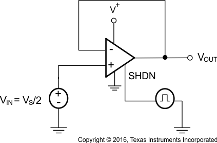 Figure 44. Turnon Time
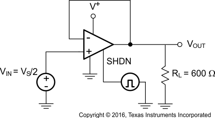 Figure 45. Turnoff Time
