-
LMV61x Single, Dual, and Quad, 1.4-MHz, Low-Power, General-Purpose 1.8-V Operational Amplifiers
- 1 Features
- 2 Applications
- 3 Description
- 4 Revision History
- 5 Pin Configuration and Functions
-
6 Specifications
- 6.1 Absolute Maximum Ratings
- 6.2 ESD Ratings
- 6.3 Recommended Operating Conditions
- 6.4 Thermal Information
- 6.5 Electrical Characteristics - 1.8 V (DC)
- 6.6 Electrical Characteristics - 1.8 V (AC)
- 6.7 Electrical Characteristics - 2.7 V (DC)
- 6.8 Electrical Characteristics - 2.7 V (AC)
- 6.9 Electrical Characteristics - 5 V (DC)
- 6.10 Electrical Characteristics - 5 V (AC)
- 6.11 Typical Characteristics
- 7 Detailed Description
- 8 Application and Implementation
- 9 Power Supply Recommendations
- 10Layout
- 11Device and Documentation Support
- 12Mechanical, Packaging, and Orderable Information
- IMPORTANT NOTICE
パッケージ・オプション
メカニカル・データ(パッケージ|ピン)
サーマルパッド・メカニカル・データ
発注情報
LMV61x Single, Dual, and Quad, 1.4-MHz, Low-Power, General-Purpose 1.8-V Operational Amplifiers
1 Features
- Supply Values: 1.8 V (Typical)
- Ensured 1.8-V, 2.7-V, and 5-V Specifications
- Output Swing:
- 80 mV From Rail With 600-Ω Load
- 30 mV From Rail With 2-kΩ Load
- VCM = 200 mV Beyond Rails
- 100-µA Supply Current (Per Channel)
- 1.4-MHz Gain Bandwidth Product
- Maximum VOS = 4 mV
- Temperature Range: −40°C to +125°C
- Create a Custom Design Using the LMV61x With the WEBENCH® Power Designer
2 Applications
- Consumer Communication
- Consumer Computing
- PDAs
- Audio Pre-Amplifiers
- Portable or Battery-Powered Electronic Equipment
- Supply Current Monitoring
- Battery Monitoring
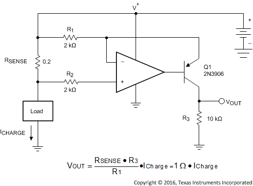
Typical Application

3 Description
The LMV61x devices are single, dual, and quad low-voltage, low-power operational amplifiers (op amps). They are designed specifically for low-voltage, general-purpose applications. Other important product characteristics are, rail-to-rail input or output, low supply voltage of 1.8 V and wide temperature range. The LMV61x input common mode extends
200 mV beyond the supplies and the output can swing rail-to-rail unloaded and within 30 mV with 2-kΩ load at 1.8-V supply. The LMV61x achieves a gain bandwidth of 1.4 MHz while drawing 100-µA (typical) quiescent current.
The industrial-plus temperature range of −40°C to 125°C allows the LMV61x to accommodate a broad range of extended environment applications.
The LMV611 is offered in the tiny 5-pin SC70 package, the LMV612 in space-saving 8-pin VSSOP and SOIC packages, and the LMV614 in 14-pin TSSOP and SOIC packages. These small package amplifiers offer an ideal solution for applications requiring minimum PCB footprint. Applications with area constrained PCB requirements include portable and battery-operated electronics.
Device Information(1)
| PART NUMBER | PACKAGE | BODY SIZE (NOM) |
|---|---|---|
| LMV611 | SOT-23 (5) | 2.92 mm × 1.60 mm |
| SC70 (5) | 2.00 mm × 1.25 mm | |
| LMV612 | VSSOP (8) | 3.00 mm × 3.00 mm |
| SOIC (8) | 4.90 mm × 3.91 mm | |
| LMV614 | TSSOP (14) | 5.00 mm × 4.40 mm |
| SOIC (14) | 8.64 mm × 3.90 mm |
- For all available packages, see the orderable addendum at the end of the data sheet.
4 Revision History
Changes from C Revision (July 2016) to D Revision
- Added links for WEBENCH Go
- Changed Slew Rate vs Supply title to reflect LMV611 and LMV614 onlyGo
- Added Slew Rate vs Supply Graph for LMV612 only Go
Changes from B Revision (March 2013) to C Revision
- Added ESD Ratings table, Feature Description section, Device Functional Modes, Application and Implementation section, Power Supply Recommendations section, Layout section, Device and Documentation Support section, and Mechanical, Packaging, and Orderable Information sectionGo
- Changed values in the Thermal Information table to align with JEDEC standardsGo
Changes from A Revision (March 2012) to B Revision
- Changed layout of National Semiconductor data sheet to TI formatGo
5 Pin Configuration and Functions

Pin Functions – LMV611
| PIN | TYPE(1) | DESCRIPTION | |
|---|---|---|---|
| NO. | NAME | ||
| 1 | +IN | I | Noninverting input |
| 2 | V– | P | Negative supply input |
| 3 | –IN | I | Inverting input |
| 4 | OUTPUT | O | Output |
| 5 | V+ | P | Positive supply input |

Pin Functions – LMV612
| PIN | TYPE(1) | DESCRIPTION | |
|---|---|---|---|
| NO. | NAME | ||
| 1 | OUT A | O | Output A |
| 2 | –IN A | I | Inverting input A |
| 3 | +IN A | I | Noninverting input A |
| 4 | V– | P | Negative supply input |
| 5 | +IN B | I | Noninverting input B |
| 6 | –IN B | I | Inverting input B |
| 7 | OUT B | O | Output B |
| 8 | V+ | P | Positive supply input |

Pin Functions – LMV614
| PIN | TYPE(1) | DESCRIPTION | |
|---|---|---|---|
| NO. | NAME | ||
| 1 | OUT A | O | Output A |
| 2 | IN A– | I | Inverting input A |
| 3 | IN A+ | I | Noninverting input A |
| 4 | V+ | P | Positive supply input |
| 5 | IN B+ | I | Noninverting input B |
| 6 | IN B– | I | Inverting input B |
| 7 | OUT B | O | Output B |
| 8 | OUT C | O | Output C |
| 9 | IN C– | I | Inverting input C |
| 10 | IN C+ | I | Noninverting input C |
| 11 | V– | P | Negative supply input |
| 12 | IN D+ | I | Noninverting input D |
| 13 | IN D– | I | Inverting input D |
| 14 | OUT D | O | Output D |