JAJSAM4D September   2007  – August 2016 LMV641

PRODUCTION DATA.  

  1. 特長
  2. アプリケーション
  3. 概要
  4. 改訂履歴
  5. Pin Configuration and Functions
  6. Specifications
    1. 6.1 Absolute Maximum Ratings
    2. 6.2 ESD Ratings
    3. 6.3 Recommended Operating Conditions
    4. 6.4 Thermal Information
    5. 6.5 DC Electrical Characteristics: 2.7 V
    6. 6.6 DC Electrical Characteristics: 10 V
    7. 6.7 Typical Characteristics
  7. Detailed Description
    1. 7.1 Overview
    2. 7.2 Functional Block Diagram
    3. 7.3 Feature Description
      1. 7.3.1 Low-Voltage and Low-Power Operation
      2. 7.3.2 Wide Bandwidth
      3. 7.3.3 Low Input Referred Noise
      4. 7.3.4 Ground Sensing and Rail-to-Rail Output
      5. 7.3.5 Small Size
    4. 7.4 Device Functional Modes
      1. 7.4.1 Stability of Op Amp Circuits
        1. 7.4.1.1 In The Loop Compensation
        2. 7.4.1.2 Compensation by External Resistor
  8. Application and Implementation
    1. 8.1 Application Information
    2. 8.2 Typical Applications
      1. 8.2.1 High-Gain, Low-Power Inverting Amplifiers
        1. 8.2.1.1 Design Requirements
        2. 8.2.1.2 Detailed Design Procedure
        3. 8.2.1.3 Application Curve
      2. 8.2.2 Anisotropic Magnetoresistive Sensor
        1. 8.2.2.1 Design Requirements
        2. 8.2.2.2 Detailed Design Procedure
          1. 8.2.2.2.1 Gain Error and Bandwidth Consideration if Using an Analog to Digital Converter
      3. 8.2.3 Voiceband Filter
  9. Power Supply Recommendations
  10. 10Layout
    1. 10.1 Layout Guidelines
    2. 10.2 Layout Example
  11. 11デバイスおよびドキュメントのサポート
    1. 11.1 デバイス・サポート
      1. 11.1.1 開発サポート
    2. 11.2 ドキュメントのサポート
      1. 11.2.1 関連資料
    3. 11.3 ドキュメントの更新通知を受け取る方法
    4. 11.4 コミュニティ・リソース
    5. 11.5 商標
    6. 11.6 静電気放電に関する注意事項
    7. 11.7 Glossary
  12. 12メカニカル、パッケージ、および注文情報

パッケージ・オプション

メカニカル・データ(パッケージ|ピン)
サーマルパッド・メカニカル・データ
発注情報

10 Layout

10.1 Layout Guidelines

To properly bypass the power supply, several locations on a printed circuit board need to be considered. A 6.8 µF or greater tantalum capacitor should be placed at the point where the power supply for the amplifier is introduced onto the board. Another 0.1-µF ceramic capacitor should be placed as close as possible to the power supply pin of the amplifier. If the amplifier is operated in a single power supply, only the V+ pin needs to be bypassed with a 0.1-µF capacitor. If the amplifier is operated in a dual power supply, both V+ and V− pins need to be bypassed. It is good practice to use a ground plane on a printed-circuit board to provide all components with a low-inductive ground connection.

10.2 Layout Example
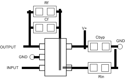
LMV641 LMV641_pcb.gif Figure 47. LMV641 Layout Example