SNOSB45F February 2010 – January 2016 LMV7231
PRODUCTION DATA.
- 1 Features
- 2 Applications
- 3 Description
- 4 Revision History
- 5 Pin Configuration and Functions
- 6 Specifications
- 7 Detailed Description
- 8 Application and Implementation
- 9 Power Supply Recommendations
- 10Layout
- 11Device and Documentation Support
- 12Mechanical, Packaging, and Orderable Information
パッケージ・オプション
メカニカル・データ(パッケージ|ピン)
- RTW|24
サーマルパッド・メカニカル・データ
- RTW|24
発注情報
10 Layout
10.1 Layout Guidelines
Proper grounding and the use of a ground plane helps to ensure the specified performance of the LMV7231. Minimizing trace lengths, reducing unwanted parasitic capacitance, and using surface-mount components also helps. Comparators are very sensitive to input noise.
- Use a printed-circuit-board with a good, unbroken low-inductance ground plane.
- Place a decoupling capacitor (0.1-µF ceramic surface mount capacitor) as close to V+ pin as possible.
- On the inputs and the outputs, keep lead lengths and the divider resistors as short possible to avoid noise pick-up.
The DAP pad is connected to the bottom of the die and is not designed to carry current. The DAP thermal pad must be connected directly to the GND pin to avoid noise and possible voltage gradients. The primary grounding pin is the GND pin.
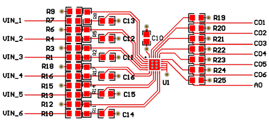
10.2 Layout Example
 Figure 41. Example Layout