SNOSB45F February 2010 – January 2016 LMV7231
PRODUCTION DATA.
- 1 Features
- 2 Applications
- 3 Description
- 4 Revision History
- 5 Pin Configuration and Functions
- 6 Specifications
- 7 Detailed Description
- 8 Application and Implementation
- 9 Power Supply Recommendations
- 10Layout
- 11Device and Documentation Support
- 12Mechanical, Packaging, and Orderable Information
パッケージ・オプション
メカニカル・データ(パッケージ|ピン)
- RTW|24
サーマルパッド・メカニカル・データ
- RTW|24
発注情報
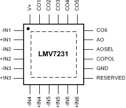
5 Pin Configuration and Functions
RTW Package
24-Pin WQFN
Top View

Pin Functions
| PIN | TYPE | DESCRIPTION | |
|---|---|---|---|
| NO. | NAME | ||
| 1 | –IN1 | Analog Input | Negative input for window comparator 1 |
| 2 | +IN1 | Analog Input | Positive input for window comparator 1 |
| 3 | –IN2 | Analog Input | Negative input for window comparator 2 |
| 4 | +IN2 | Analog Input | Positive input for window comparator 2 |
| 5 | –IN3 | Analog Input | Negative input for window comparator 3 |
| 6 | +IN3 | Analog Input | Positive input for window comparator 3 |
| 7 | –IN4 | Analog Input | Negative input for window comparator 4 |
| 8 | +IN4 | Analog Input | Positive input for window comparator 4 |
| 9 | –IN5 | Analog Input | Negative input for window comparator 5 |
| 10 | +IN5 | Analog Input | Positive input for window comparator 5 |
| 11 | –IN6 | Analog Input | Negative input for window comparator 6 |
| 12 | +IN6 | Analog Input | Positive input for window comparator 6 |
| 13 | RESERVED | Digital Input | Connect to GND |
| 14 | GND | Power | Ground reference pin for the power supply voltage |
| 15 | COPOL | Digital Input | The state of this pin determines whether the CO1-CO6 pins are active “HIGH” or “LOW”. When tied LOW the CO1-CO6 outputs go LOW to indicate an out-of-window comparison. |
| 16 | AOSEL | Digital Input | The state of this pin determines whether the AO pin is active on an overvoltage or undervoltage event. When tied LOW the AO output is active upon an overvoltage event. |
| 17 | AO | Open-Drain NMOS Digital Output | This output is the ANDED combination of either the overvoltage comparator outputs or the undervoltage comparator outputs and is controlled by the state of the AOSEL. AO pin is active-low. |
| 18 | CO6 | Open-Drain NMOS Digital Output | Window comparator 6 NMOS open-drain output |
| 19 | CO5 | Open-Drain NMOS Digital Output | Window comparator 5 NMOS open-drain output |
| 20 | CO4 | Open-Drain NMOS Digital Output | Window comparator 4 NMOS open-drain output |
| 21 | CO3 | Open-Drain NMOS Digital Output | Window comparator 3 NMOS open-drain output |
| 22 | CO2 | Open-Drain NMOS Digital Output | Window comparator 2 NMOS open-drain output |
| 23 | CO1 | Open-Drain NMOS Digital Output | Window comparator 1 NMOS open-drain output |
| 24 | V+ | Power | Power supply pin |
| DAP | DAP | Thermal Pad | Die Attach Paddle (DAP). Connect to GND. |