JAJSF92O September   2000  – April 2018 LMV7235 , LMV7239

PRODUCTION DATA.  

  1. 特長
  2. アプリケーション
  3. 概要
    1.     Device Images
      1.      消費電流と電源電圧との関係
      2.      伝搬遅延とオーバードライブ
  4. 改訂履歴
  5. Pin Configuration and Functions
    1.     Pin Functions
  6. Specifications
    1. 6.1 Absolute Maximum Ratings
    2. 6.2 ESD Ratings
    3. 6.3 Recommended Operating Conditions
    4. 6.4 Thermal Information
    5. 6.5 Electrical Characteristics, 2.7 V
    6. 6.6 Electrical Characteristics, 5 V
    7. 6.7 Typical Characteristics
  7. Detailed Description
    1. 7.1 Overview
    2. 7.2 Functional Block Diagram
    3. 7.3 Feature Description
      1. 7.3.1 Input Stage
      2. 7.3.2 Output Stage: LMV7239
      3. 7.3.3 Output Stage: LMV7235
    4. 7.4 Device Functional Modes
      1. 7.4.1 Capacitive and Resistive Loads
      2. 7.4.2 Noise
      3. 7.4.3 Hysteresis
        1. 7.4.3.1 Inverting Comparator With Hysteresis
        2. 7.4.3.2 Non-Inverting Comparator With Hysteresis
      4. 7.4.4 Zero Crossing Detector
        1. 7.4.4.1 Zero Crossing Detector With Hysteresis
      5. 7.4.5 Threshold Detector
  8. Application and Implementation
    1. 8.1 Application Information
    2. 8.2 Typical Applications
      1. 8.2.1 Square Wave Oscillator
        1. 8.2.1.1 Design Requirements
        2. 8.2.1.2 Detailed Design Procedure
        3. 8.2.1.3 Application Curves
      2. 8.2.2 Crystal Oscillator
      3. 8.2.3 Infrared (IR) Receiver
      4. 8.2.4 Window Detector
  9. Power Supply Recommendations
  10. 10Layout
    1. 10.1 Layout Guidelines
    2. 10.2 Layout Example
  11. 11デバイスおよびドキュメントのサポート
    1. 11.1 デバイス・サポート
      1. 11.1.1 開発サポート
    2. 11.2 ドキュメントのサポート
      1. 11.2.1 関連資料
    3. 11.3 関連リンク
    4. 11.4 ドキュメントの更新通知を受け取る方法
    5. 11.5 コミュニティ・リソース
    6. 11.6 商標
    7. 11.7 静電気放電に関する注意事項
    8. 11.8 Glossary
  12. 12メカニカル、パッケージ、および注文情報

パッケージ・オプション

メカニカル・データ(パッケージ|ピン)
サーマルパッド・メカニカル・データ
発注情報

Inverting Comparator With Hysteresis

The inverting comparator with hysteresis requires a three resistor network that is referenced to the supply voltage V+ of the comparator as shown in Figure 19. When VIN at the inverting input is less than VA, the voltage at the noninverting node of the comparator (VIN< VA), the output voltage is high (for simplicity assume VO switches as high as V+). The three network resistors can be represented as R1//R3 in series with R2.
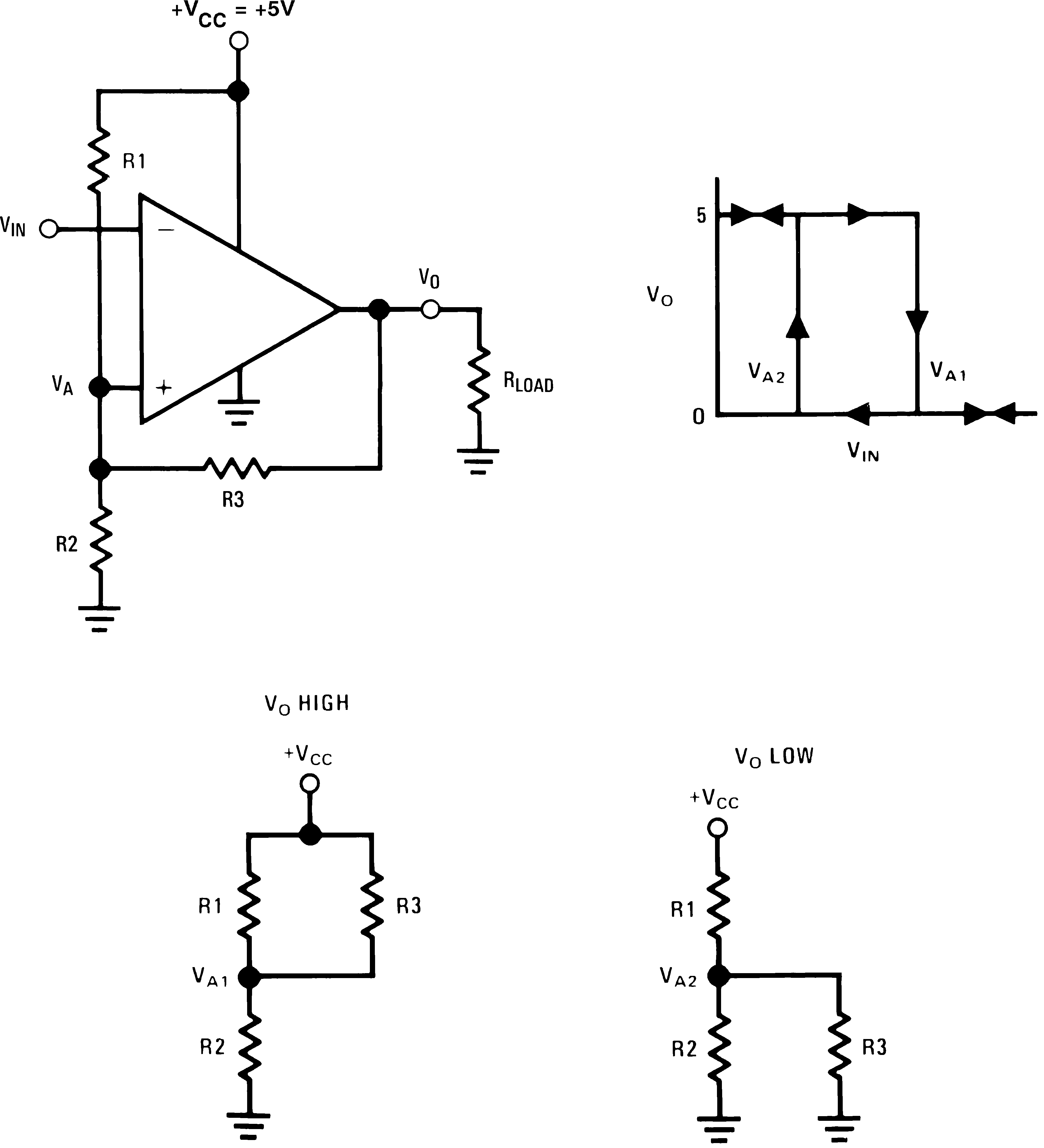
LMV7235 LMV7239 20201334.pngFigure 19. Inverting Comparator With Hysteresis

The lower input trip voltage VA1 is defined as:

Equation 1. VA1 = VCCR2 / [(R1 // R3) + R2)]

When VIN is greater than VA, the output voltage is low or very close to ground. In this case the three network resistors can be presented as R2 // R3 in series with R1.

The upper trip voltage VA2 is defined as:

Equation 2. VA2 = VCC (R2 // R3) / [(R1 ) + (R2 // R3)]

The total hysteresis provided by the network is defined as ΔVA = VA1 - VA2.

Equation 3. LMV7235 LMV7239 eq01_snoscz2.gif