SNOSD09 September   2015 LMV7275-Q1

PRODUCTION DATA.  

  1. Features
  2. Applications
  3. Description
  4. Revision History
  5. Pin Configuration and Functions
  6. Specifications
    1. 6.1  Absolute Maximum Ratings
    2. 6.2  ESD Ratings LMV7275-Q1
    3. 6.3  Recommended Operating Conditions
    4. 6.4  Thermal Information
    5. 6.5  1.8-V Electrical Characteristics
    6. 6.6  1.8-V AC Electrical Characteristics
    7. 6.7  2.7-V Electrical Characteristics
    8. 6.8  2.7-V AC Electrical Characteristics
    9. 6.9  5-V Electrical Characteristics
    10. 6.10 5-V AC Electrical Characteristics
    11. 6.11 Typical Characteristics
  7. Detailed Description
    1. 7.1 Overview
    2. 7.2 Functional Block Diagram
    3. 7.3 Feature Description
      1. 7.3.1 Rail-to-Rail Input Stage
      2. 7.3.2 Output Stage
    4. 7.4 Device Functional Modes
      1. 7.4.1 Capacitive and Resistive Loads
      2. 7.4.2 Noise
      3. 7.4.3 Hysteresis
        1. 7.4.3.1 Non-inverting Comparator With Hysteresis
        2. 7.4.3.2 Inverting Comparator With Hysteresis
      4. 7.4.4 Zero Crossing Detector
        1. 7.4.4.1 Zero Crossing Detector With Hysteresis
      5. 7.4.5 Threshold Detector
      6. 7.4.6 Universal Logic Level Shifter
      7. 7.4.7 OR'ING the Output
  8. Application and Implementation
    1. 8.1 Application Information
    2. 8.2 Typical Applications
      1. 8.2.1 Square Wave Oscillator
        1. 8.2.1.1 Design Requirements
        2. 8.2.1.2 Detailed Design Procedure
        3. 8.2.1.3 Application Curve
      2. 8.2.2 Positive Peak Detector
      3. 8.2.3 Negative Peak Detector
      4. 8.2.4 Window Detector
  9. Power Supply Recommendations
  10. 10Layout
    1. 10.1 Layout Guidelines
      1. 10.1.1 Circuit Techniques for Avoiding Oscillations in Comparator Applications
    2. 10.2 Layout Example
  11. 11Device and Documentation Support
    1. 11.1 Device Support
      1. 11.1.1 Development Support
    2. 11.2 Documentation Support
      1. 11.2.1 Related Documentation
    3. 11.3 Community Resources
    4. 11.4 Trademarks
    5. 11.5 Electrostatic Discharge Caution
    6. 11.6 Glossary
  12. 12Mechanical, Packaging, and Orderable Information

パッケージ・オプション

メカニカル・データ(パッケージ|ピン)
サーマルパッド・メカニカル・データ
発注情報

5 Pin Configuration and Functions

DGK Package
5-Pin SC70
Top View
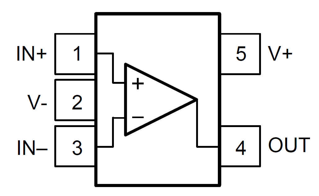
LMV7275-Q1 pinout_sot_south.gif

Pin Functions

PIN I/O DESCRIPTION
NAME SC70
IN+ 1 I Non-Inverting Input
V- 2 P Negative Supply Voltage
IN- 3 I Inverting Input
OUT 4 O Output
V+ 5 P Positive Supply Voltage