JAJSAU5C August 2008 – November 2015 LMV831 , LMV832 , LMV834
PRODUCTION DATA.
6.7 Typical Characteristics
At TA = 25°C, RL = 10 kΩ, V+ = 3.3 V, V− = 0 V, Unless otherwise specified.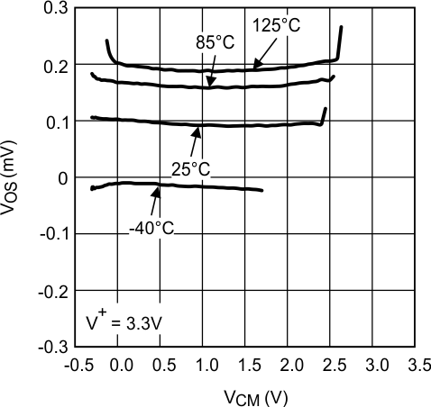 Figure 1. VOS vs VCM at V+ = 3.3 V
 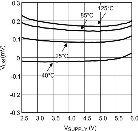 Figure 3. VOS vs Supply Voltage
 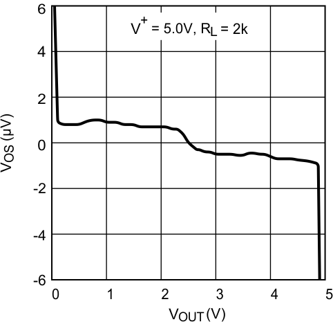 Figure 5. VOS vs VOUT
 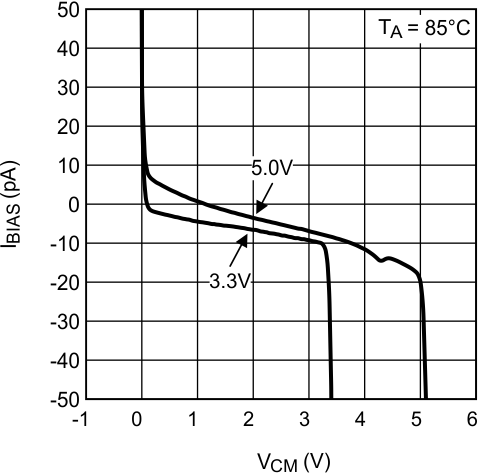 Figure 7. Input Bias Current vs VCM at 85°C
 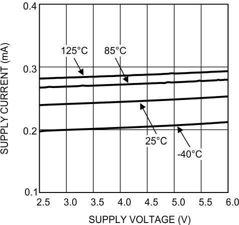 Figure 9. Supply Current vs Supply Voltage Single LMV831
 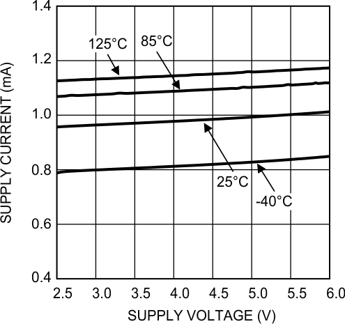 Figure 11. Supply Current vs Supply Voltage Quad LMV834
 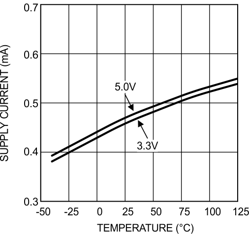 Figure 13. Supply Current vs Temperature Dual LMV832
 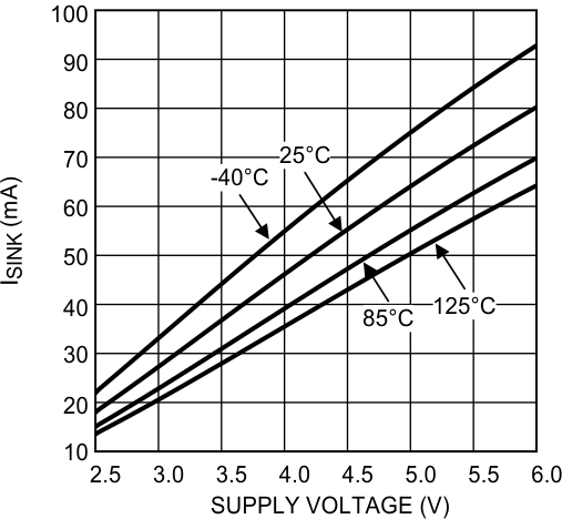 Figure 15. Sinking Current vs Supply Voltage
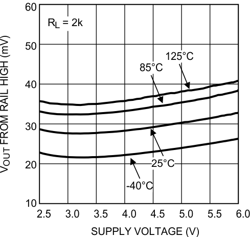
RL = 2 kΩ
Figure 17. Output Swing High vs Supply Voltage 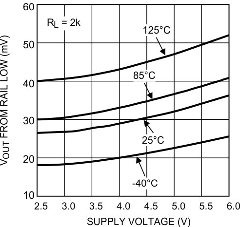
RL = 2 kΩ
Figure 19. Output Swing Low vs Supply Voltage 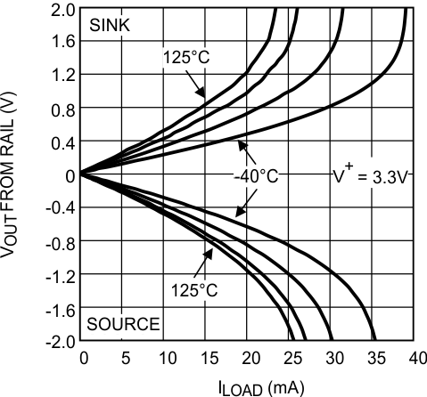 Figure 21. Output Voltage Swing vs Load Current at V+ = 3.3 V
 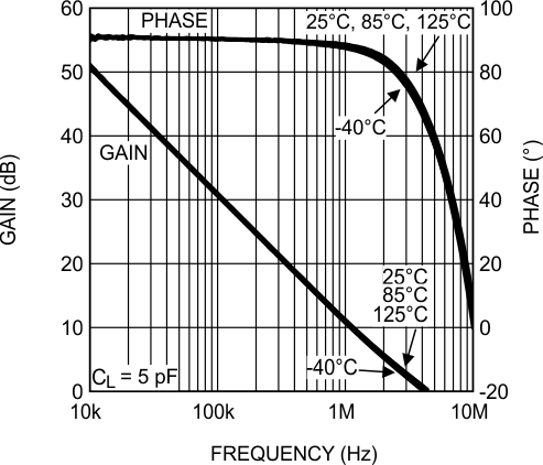 Figure 23. Open-Loop Frequency Response vs Temperature
 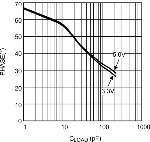 Figure 25. Phase Margin vs Capacitive Load
 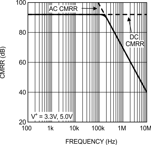 Figure 27. CMRR vs Frequency
 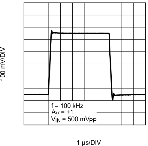 Figure 29. Large Signal Step Response With Gain = 1
 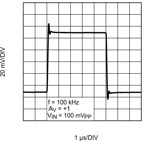 Figure 31. Small Signal Step Response With Gain = 1
 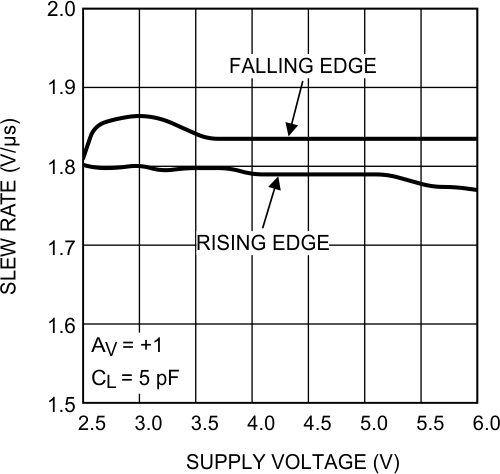 Figure 33. Slew Rate vs Supply Voltage
 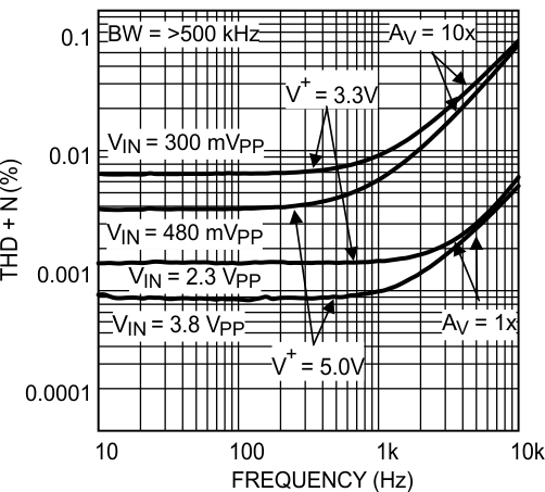 Figure 35. THD+N vs Frequency
 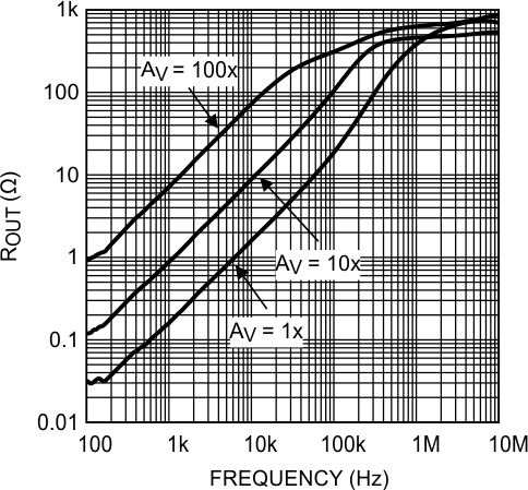 Figure 37. ROUT vs Frequency
 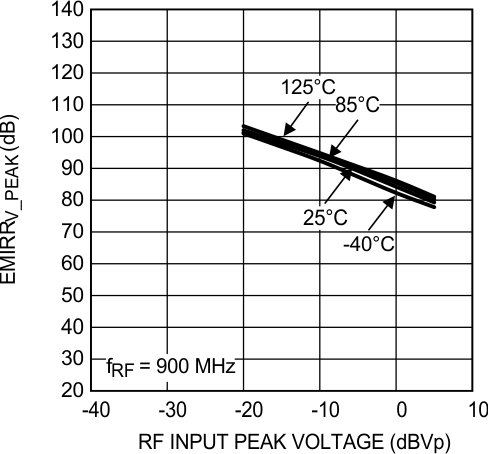 Figure 39. EMIRR IN+ vs Power at 900 MHz
 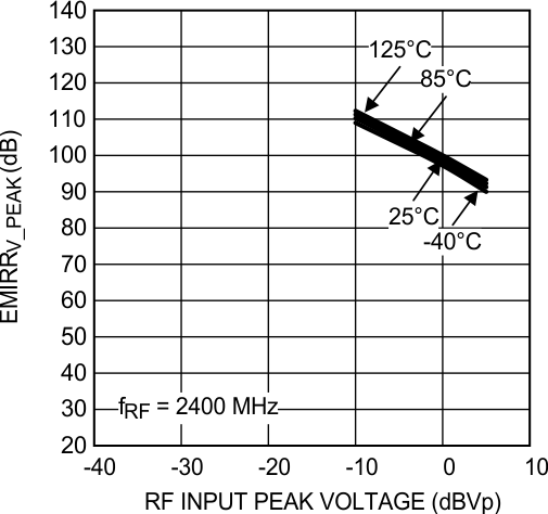 Figure 41. EMIRR IN+ vs Power at 2400 MHz
 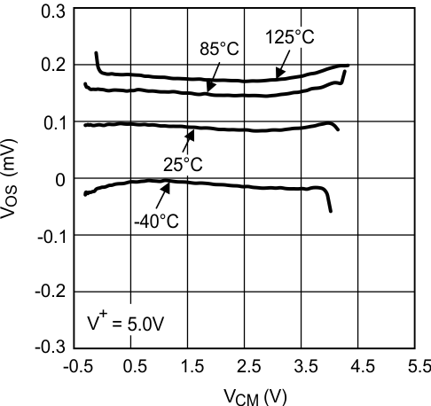 Figure 2. VOS vs VCM at V+ = 5 V
 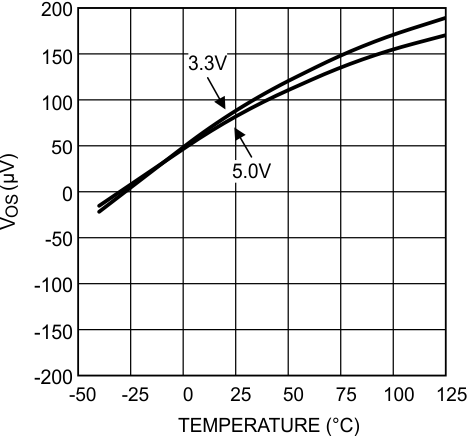 Figure 4. VOS vs Temperature
 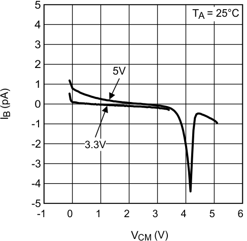 Figure 6. Input Bias Current vs VCM at 25°C
 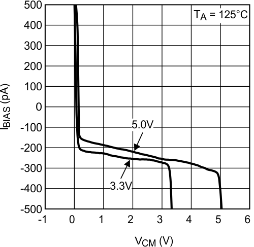 Figure 8. Input Bias Current vs VCM at 125°C
 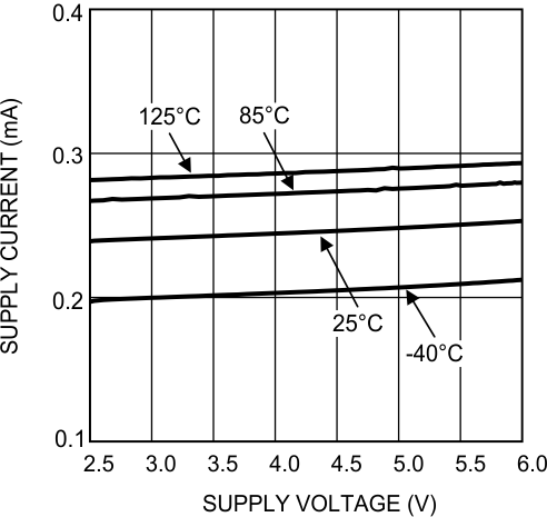 Figure 10. Supply Current vs Supply Voltage Dual LMV832
 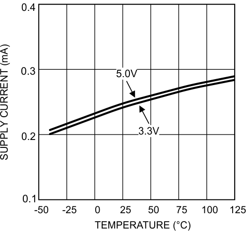 Figure 12. Supply Current vs Temperature Single LMV831
 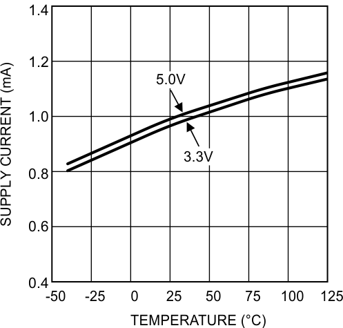 Figure 14. Supply Current vs Temperature Quad LMV834
 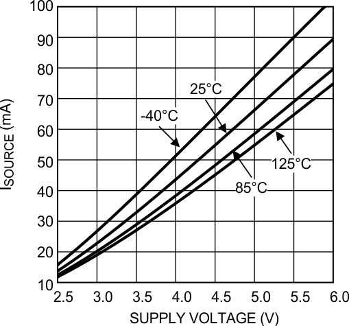 Figure 16. Sourcing Current vs Supply Voltage
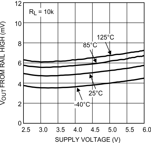
RL = 10 kΩ
Figure 18. Output Swing High vs Supply Voltage 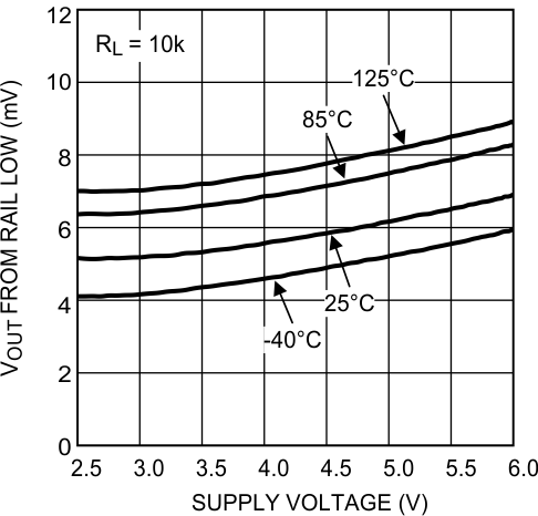
RL = 10 kΩ
Figure 20. Output Swing Low vs Supply Voltage 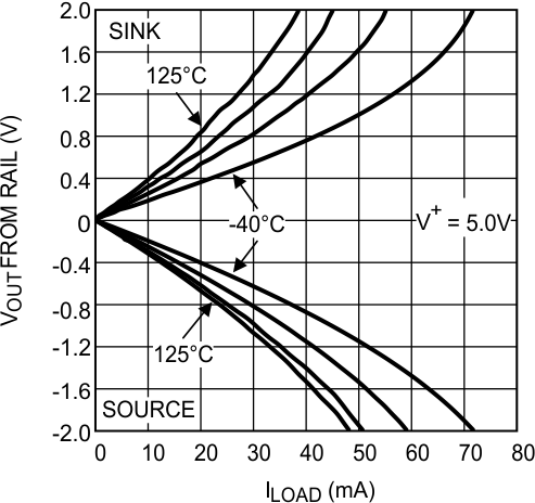 Figure 22. Output Voltage Swing vs Load Current at V+ = 5 V
 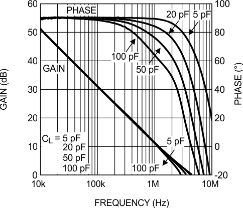 Figure 24. Open-Loop Frequency Response vs Load Conditions
 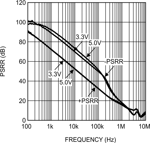 Figure 26. PSRR vs Frequency
 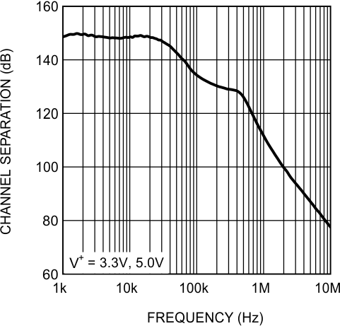 Figure 28. Channel Separation vs Frequency
 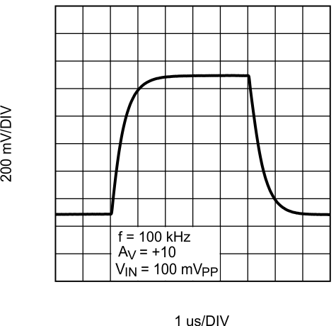 Figure 30. Large Signal Step Response With Gain = 10
 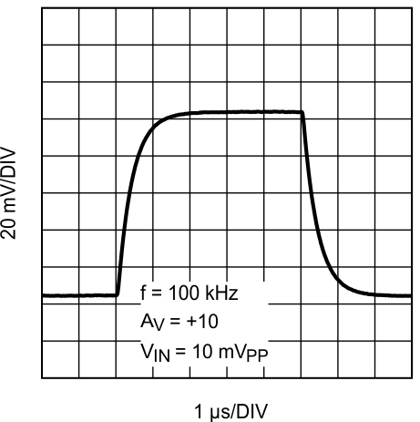 Figure 32. Small Signal Step Response With Gain = 10
 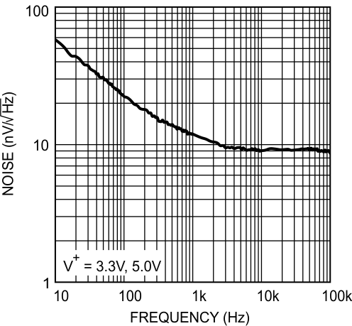 Figure 34. Input Voltage Noise vs Frequency
 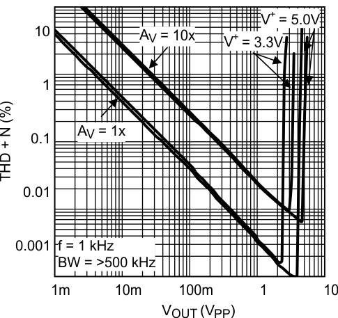 Figure 36. THD+N vs Amplitude
 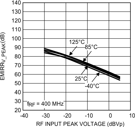 Figure 38. EMIRR IN+ vs Power at 400 MHz
 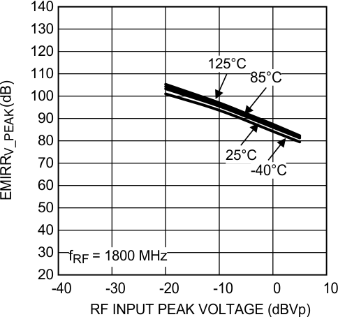 Figure 40. EMIRR IN+ vs Power at 1800 MHz
 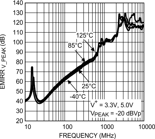 Figure 42. EMIRR IN+ vs Frequency