SNOS993P November 2001 – April 2017 LMV931-N , LMV932-N , LMV934-N
PRODUCTION DATA.
- 1 Features
- 2 Applications
- 3 Description
- 4 Revision History
- 5 Pin Configuration and Functions
-
6 Specifications
- 6.1 Absolute Maximum Ratings
- 6.2 ESD Ratings (Commercial)
- 6.3 Recommended Operating Ratings
- 6.4 Thermal Information
- 6.5 DC Electrical Characteristics 1.8 V
- 6.6 AC Electrical Characteristics 1.8 V
- 6.7 DC Electrical Characteristics 2.7 V
- 6.8 AC Electrical Characteristics 2.7 V
- 6.9 Electrical Characteristics 5 V DC
- 6.10 AC Electrical Characteristics 5 V
- 6.11 Typical Characteristics
- 7 Detailed Description
- 8 Application and Implementation
- 9 Power Supply Recommendations
- 10Layout
- 11Device and Documentation Support
- 12Mechanical, Packaging, and Orderable Information
1 Features
- Typical 1.8-V Supply Values; Unless Otherwise Noted
- Specified at 1.8 V, 2.7 V and 5 V
- Output Swing
- With 600-Ω Load 80 mV from Rail
- With 2-kΩ Load 30 mV from Rail
- VCM 200 mV Beyond Rails
- Supply Current (per Channel) 100 μA
- Gain Bandwidth Product 1.4 MHz
- Maximum VOS 4 mV
- Ultra Tiny Packages
- Temperature Range −40°C to +125°C
- Create a Custom Design Using the LMV93x-N With the WEBENCH® Power Designer
2 Applications
- Phones
- Tablets
- Wearables
- Health Monitoring
- Portable and Battery-Powered Electronic Equipment
- Battery Monitoring
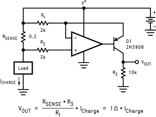
High-Side Current Sense Amplifier

3 Description
The LMV93x-N family (LMV931-N single, LMV932-N dual and LMV934-N quad) are low-voltage, low-power operational amplifiers. The LMV93x-N family operates from 1.8-V to 5.5-V supply voltages and have rail-to-rail input and output. The input common-mode voltage extends 200 mV beyond the supplies which enables user enhanced functionality beyond the supply voltage range. The output can swing rail-to-rail unloaded and within 105 mV from the rail with 600-Ω load at 1.8-V supply. The LMV93x-N devices are optimized to work at 1.8 V, which make them ideal for portable two-cell, battery-powered systems and single-cell Li-Ion systems.
LMV93x-N devices exhibit an excellent speed-power ratio, achieving 1.4-MHz gain bandwidth product at 1.8-V supply voltage with very low supply current. The LMV93x-N devices can drive a 600-Ω load and up to 1000-pF capacitive load with minimal ringing. These devices also have a high DC gain of 101 dB, making them suitable for low-frequency applications.
The single LMV93x-N is offered in space-saving 5-pin SC70 and SOT-23 packages. The dual LMV932-N are in 8-pin VSSOP and SOIC packages and the quad LMV934-N are in 14-pin TSSOP and SOIC packages. These small packages are ideal solutions for area constrained PC boards and portable electronics such as mobile phones and tablets.
Device Information(1)
| PART NUMBER | PACKAGE | BODY SIZE (NOM) |
|---|---|---|
| LMV931-N | SOT-23 (5) | 2.90 mm × 1.60 mm |
| SC-70 (5) | 2.00 mm × 1.25 mm | |
| LMV932-N | VSSOP (8) | 3.00 mm × 3.00 mm |
| SOIC (8) | 4.90 mm × 3.91 mm | |
| LMV934-N | TSSOP (8) | 5.00 mm × 4.40 mm |
| SOIC (14) | 8.60 mm × 3.90 mm |
- For all available packages, see the orderable addendum at the end of the datasheet.