SNAS236G October 2005 – January 2016 LMX2485 , LMX2485E
PRODUCTION DATA.
- 1 Features
- 2 Applications
- 3 Description
- 4 Revision History
- 5 Pin Configuration and Functions
- 6 Specifications
- 7 Parameter Measurement Information
-
8 Detailed Description
- 8.1 Overview
- 8.2 Functional Block Diagram
- 8.3
Feature Description
- 8.3.1 TCXO, Oscillator Buffer, and R Counter
- 8.3.2 Phase Detector
- 8.3.3 Charge Pump
- 8.3.4 Loop Filter
- 8.3.5 N Counters and High Frequency Input Pins
- 8.3.6 Digital Lock Detect Operation
- 8.3.7 Cycle Slip Reduction and Fastlock
- 8.3.8 Fractional Spur and Phase Noise Controls
- 8.4 Device Functional Modes
- 8.5 Programming
- 8.6
Register Maps
- 8.6.1 R0 Register
- 8.6.2 R1 Register
- 8.6.3 R2 Register
- 8.6.4 R3 Register
- 8.6.5
R4 Register
- 8.6.5.1 MUX[3:0] Frequency Out and Lock Detect MUX
- 8.6.5.2 IF_P—IF Prescaler
- 8.6.5.3 RF_CPP—RF PLL Charge Pump Polarity
- 8.6.5.4 IF_CPP—IF PLL Charge Pump Polarity
- 8.6.5.5 OSC_OUT Oscillator Output Buffer Enable
- 8.6.5.6 OSC2X—Oscillator Doubler Enable
- 8.6.5.7 FM[1:0]—Fractional Mode
- 8.6.5.8 DITH[1:0]—Dithering Control
- 8.6.5.9 ATPU—PLL Automatic Power Up
- 8.6.6 R5 Register
- 8.6.7 R6 Register
- 8.6.8 R7 Register
- 9 Application and Implementation
- 10Power Supply Recommendations
- 11Layout
- 12Device and Documentation Support
- 13Mechanical, Packaging, and Orderable Information
1 Features
- Quadruple Modulus Prescaler for Lower Divides
- RF PLL: 8/9/12/13 or 16/17/20/21
- IF PLL: 8/9 or 16/17
- Advanced Delta-Sigma Fractional Compensation
- 12-Bit or 22-Bit Selectable Fractional Modulus
- Up to 4th Order Programmable Delta-Sigma Modulator
- Features for Improved Lock Time
- Fastlock / Cycle Slip Reduction With Integrated Time-Out Counter Which Requires Only a Single-Word Write
- Wide Operating Range
- LMX2485 RF PLL: 500 MHz to 3.0 GHz
- LMX2485E RF PLL: 50 MHz to 3.0 GHz
- Useful Features
- Digital Lock Detect Output
- Hardware and Software Power-Down Control
- On-Chip Input Frequency Doubler.
- RF Phase Detector Frequency up to 50 MHz
- 2.5 to 3.6 V Operation With ICC = 5.0 mA
2 Applications
- Cellular Phones and Base Stations
- Direct Digital Modulation Applications
- Satellite and Cable TV Tuners
- WLAN Standards
3 Description
The LMX2485 device is a low power, high performance delta-sigma fractional-N PLL with an auxiliary integer-N PLL. The device is fabricated using Texas Instruments' advanced process.
With delta-sigma architecture, fractional spurs at lower offset frequencies are pushed to higher frequencies outside the loop bandwidth. The ability to push close in spur and phase noise energy to higher frequencies is a direct function of the modulator order. Unlike analog compensation, the digital feedback technique used in the LMX2485 is highly resistant to changes in temperature and variations in wafer processing. The LMX2485 delta-sigma modulator is programmable up to fourth order, which allows the designer to select the optimum modulator order to fit the phase noise, spur, and lock time requirements of the system.
Serial data for programming the LMX2485 is transferred through a three-line, high-speed (20-MHz) MICROWIRE interface. The LMX2485 offers fine frequency resolution, low spurs, fast programming speed, and a single-word write to change the frequency. This makes it ideal for direct digital modulation applications, where the N-counter is directly modulated with information. The LMX2485 is available in a 24-lead 4.0 × 4.0 × 0.8 mm WQFN package.
Device Information(1)
| PART NUMBER | RF PLL Frequency | IF PLL Frequency |
|---|---|---|
| LMX2485E | 50 - 3000 MHz | 75 - 800 MHz |
| LMX2485 | 500 - 3000 MHz | 75 - 800 MHz |
- For all available packages, see the orderable addendum at the end of the data sheet.
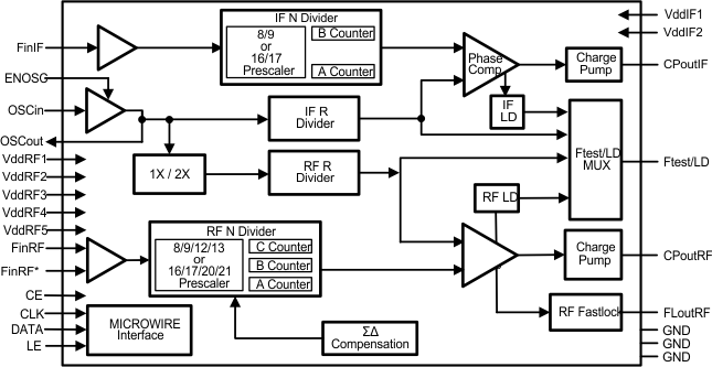
Functional Block Diagram
