SNOSB31J July 2009 – December 2014 LMX2541
PRODUCTION DATA.
- 1 Features
- 2 Applications
- 3 Description
- 4 Revision History
- 5 Device Comparison Table
- 6 Pin Configuration and Functions
- 7 Specifications
- 8 Parameter Measurement Information
-
9 Detailed Description
- 9.1 Overview
- 9.2 Functional Block Diagrams
- 9.3
Feature Description
- 9.3.1 PLL Reference Oscillator Input Pins
- 9.3.2 PLL R Divider
- 9.3.3 PLL Phase Detector and Charge Pump
- 9.3.4 PLL N Divider and Fractional Circuitry
- 9.3.5 Partially Integrated Loop Filter
- 9.3.6 Low Noise, Fully Integrated VCO
- 9.3.7 Programmable VCO Divider
- 9.3.8 Programmable RF Output Buffer
- 9.3.9 Powerdown Modes
- 9.3.10 Fastlock
- 9.3.11 Lock Detect
- 9.3.12 Current Consumption
- 9.3.13 Fractional Spurs
- 9.3.14 Impact of VCO_DIV on Fractional Spurs
- 9.3.15 PLL Phase Noise
- 9.3.16 Impact of Modulator Order, Dithering, and Larger Equivalent Fractions on Spurs and Phase Noise
- 9.3.17 Modulator Order
- 9.3.18 Programmable Output Power with On/Off
- 9.3.19 Loop Filter
- 9.3.20 Internal VCO Digital Calibration Time
- 9.4 Device Functional Modes
- 9.5 Programming
- 9.6
Register Maps
- 9.6.1
Register R7
- 9.6.1.1 Register R13
- 9.6.1.2 Register R12
- 9.6.1.3 Register R9
- 9.6.1.4 Register R8
- 9.6.1.5 Register R6
- 9.6.1.6 Register R5
- 9.6.1.7
Register R4
- 9.6.1.7.1 OSC_FREQ [7:0] -- OSCin Frequency for VCO Calibration Clocking
- 9.6.1.7.2 VCO_DIV[5:0] - VCO Divider
- 9.6.1.7.3 R3_LF[2:0] -- Value for Internal Loop Filter Resistor R3
- 9.6.1.7.4 R4_LF[2:0] -- Value for Internal Loop Filter Resistor R4
- 9.6.1.7.5 C3_LF[3:0] -- Value for C3 in the Internal Loop Filter
- 9.6.1.7.6 C4_LF[3:0] -- Value for C4 in the Internal Loop Filter
- 9.6.1.8
Register R3
- 9.6.1.8.1 MODE[1:0] -- Operational Mode
- 9.6.1.8.2 Powerdown -- Powerdown Bit
- 9.6.1.8.3 XO - Crystal Oscillator Mode Select
- 9.6.1.8.4 CPG[4:0] -- Charge Pump Current
- 9.6.1.8.5 MUX[3:0] -- Multiplexed Output for Ftest/LD Pin
- 9.6.1.8.6 CPP - Charge Pump Polarity
- 9.6.1.8.7 OSC2X-- OSCin Frequency Doubler
- 9.6.1.8.8 FDM - Extended Fractional Denominator Mode Enable
- 9.6.1.8.9 ORDER[2:0] -- Delta-Sigma Modulator Order
- 9.6.1.8.10 DITH[1:0] -- Dithering
- 9.6.1.8.11 CPT - Charge Pump TRI-STATE
- 9.6.1.8.12 DLOCK[2:0] - Controls for Digital Lock Detect
- 9.6.1.8.13 FSK - Frequency Shift Keying
- 9.6.1.9 Register R2
- 9.6.1.10 Registers R1 and R0
- 9.6.1
Register R7
-
10Application and Implementation
- 10.1
Application Information
- 10.1.1 Determining the Best Frequency Option of the LMX2541 to Use
- 10.1.2 RFout Output Power Test Setup
- 10.1.3 Phase Noise Measurement Test Setup
- 10.1.4 Input and Output Impedance Test Setup
- 10.1.5 ExtVCOin (NOT OSCin) Input Sensitivity Test Setup
- 10.1.6 OSCin Input Sensitivity Test Setup
- 10.1.7 Typical Connections
- 10.2 Typical Application
- 10.1
Application Information
- 11Power Supply Recommendations
- 12Layout
- 13Device and Documentation Support
- 14Mechanical, Packaging, and Orderable Information
パッケージ・オプション
デバイスごとのパッケージ図は、PDF版データシートをご参照ください。
メカニカル・データ(パッケージ|ピン)
- NJK|36
サーマルパッド・メカニカル・データ
発注情報
12 Layout
12.1 Layout Guidelines
12.1.1 Configuring the LMX2541 for Optimal Performance
- Determine the Channel Spacing (fCH)
- For a system that has a VCO that tunes over several frequencies, the channel spacing is the tuning increment. In the case that the VCO frequency is fixed, this channel spacing is the greatest number that divides both the VCO frequency and the OSCin frequency.
- Determine OSCin Frequency (fOSCin)
- If the OSCin frequency is not already determined, then there are several considerations. A higher frequency is generally, but not always, preferable. One reason for this is that it has a higher slew rate if it is a sine wave. Another reason is that the clock for the VCO frequency calibration is based on the OSCin frequency and in general will run faster for higher OSCin frequencies.
- Although a higher OSCin frequency is desirable, there are also reasons to use a lower frequency. If the OSCin frequency is strategically chosen, the worst case fractional spur channels might fall out of band. Also, if the OSCin frequency can be chosen such that the fractional denominator can avoid factors of 2 and/or 3, the sub-fractional spurs can be reduced.
- Determine the Phase Detector Frequency (fPD) , Charge Pump Gain (KPD) and Fractional Denominator (FDEN)
- In general, choose the highest phase detector frequency and charge pump gain, unless it leads to loop filter capacitor values that are unrealistically large for a given loop bandwidth. In this case, reducing either the phase detector frequency or the charge pump gain can yield more feasible capacitor values. Other reasons for not using the highest charge pump gain is to allow some adjustment margin to compensate for changes in the VCO gain or allow the use of Fastlock.
- For choosing the fractional denominator, start with FDEN = fPD/fCH. As discussed previously, there might be reasons to choose larger equivalent fractions.
- Design the Loop Filter
- Determine the Modulator Order
- Determine Dithering and Potential Larger Equivalent Fractional Value
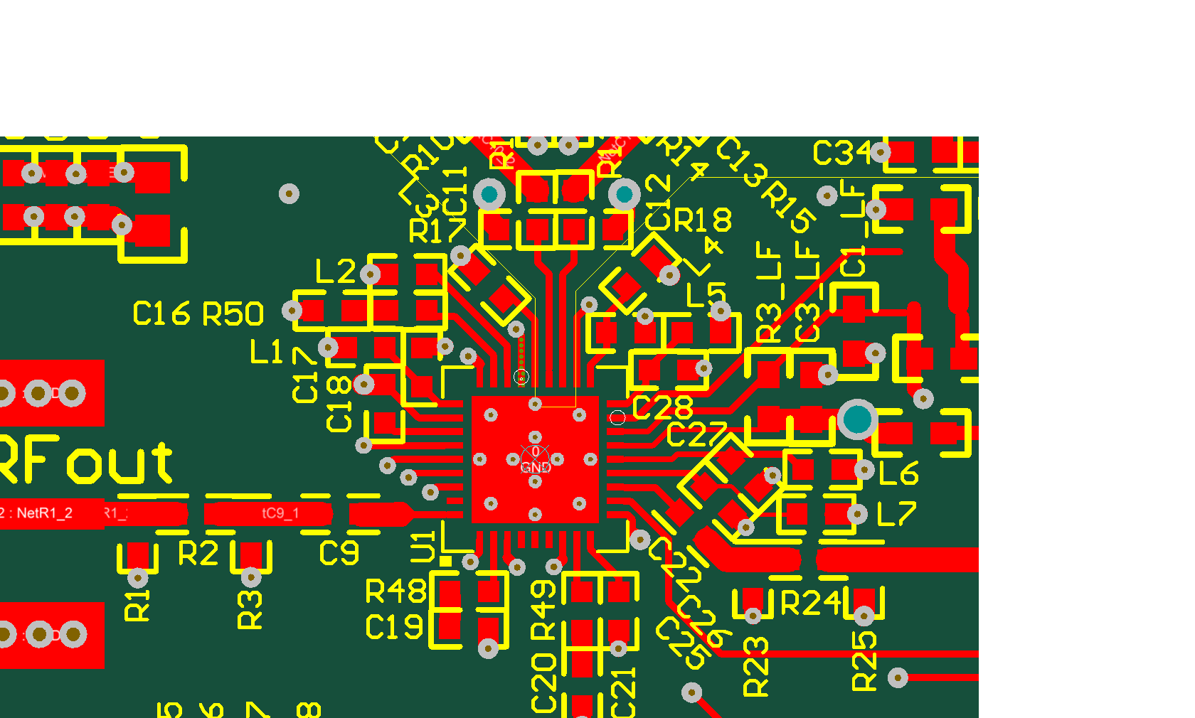
12.2 Layout Example
 Figure 35. Layout