JAJSN48B October 2021 – June 2022 LMX2571-EP
PRODUCTION DATA
- 1 特長
- 2 アプリケーション
- 3 概要
- 4 Revision History
- 5 Pin Configuration and Functions
- 6 Specifications
-
7 Detailed Description
- 7.1 Overview
- 7.2 Functional Block Diagram
- 7.3
Feature Description
- 7.3.1 Differences Between the LMX2571 and LMX2571-EP
- 7.3.2 Reference Oscillator Input
- 7.3.3 R-Dividers and Multiplier
- 7.3.4 PLL Phase Detector and Charge Pump
- 7.3.5 PLL N-Divider and Fractional Circuitry
- 7.3.6 Partially Integrated Loop Filter
- 7.3.7 Low-Noise, Fully Integrated VCO
- 7.3.8 External VCO Support
- 7.3.9 Programmable RF Output Divider
- 7.3.10 Programmable RF Output Buffer
- 7.3.11 Integrated TX, RX Switch
- 7.3.12 Power Down
- 7.3.13 Lock Detect
- 7.3.14 FSK Modulation
- 7.3.15 FastLock
- 7.3.16 Register Readback
- 7.4 Device Functional Modes
- 7.5 Programming
- 7.6
Register Maps
- 7.6.1 R60 Register (offset = 3Ch) [reset = 4000h]
- 7.6.2 R58 Register (offset = 3Ah) [reset = C00h]
- 7.6.3 R53 Register (offset = 35h) [reset = 2802h]
- 7.6.4 R47 Register (offset = 2Fh) [reset = 0h]
- 7.6.5 R46 Register (offset = 2Eh) [reset = 1Ah]
- 7.6.6 R42 Register (offset = 2Ah) [reset = 210h]
- 7.6.7 R41 Register (offset = 29h) [reset = 810h]
- 7.6.8 R40 Register (offset = 28h) [reset = 101Ch]
- 7.6.9 R39 Register (offset = 27h) [reset = 11F0h]
- 7.6.10 R35 Register (offset = 23h) [reset = 647h]
- 7.6.11 R34 Register (offset = 22h) [reset = 1000h]
- 7.6.12 R33 Register (offset = 21h) [reset = 0h]
- 7.6.13 R25 to R32 Register (offset = 19h to 20h) [reset = 0h]
- 7.6.14 R24 Register (offset = 18h) [reset = 10h]
- 7.6.15 R23 Register (offset = 17h) [reset = 10A4h]
- 7.6.16 R22 Register (offset = 16h) [reset = 8584h]
- 7.6.17 R21 Register (offset = 15h) [reset = 101h]
- 7.6.18 R20 Register (offset = 14h) [reset = 28h]
- 7.6.19 R19 Register (offset = 13h) [reset = 0h]
- 7.6.20 R18 Register (offset = 12h) [reset = 0h]
- 7.6.21 R17 Register (offset = 11h) [reset = 0h]
- 7.6.22 R9 to R16 Register (offset = 9h to 10h) [reset = 0h]
- 7.6.23 R8 Register (offset = 8h) [reset = 10h]
- 7.6.24 R7 Register (offset = 7h) [reset = 10A4h]
- 7.6.25 R6 Register (offset = 6h) [reset = 8584h]
- 7.6.26 R5 Register (offset = 5h) [reset = 101h]
- 7.6.27 R4 Register (offset = 4h) [reset = 28h]
- 7.6.28 R3 Register (offset = 3h) [reset = 0h]
- 7.6.29 R2 Register (offset = 2h) [reset = 0h]
- 7.6.30 R1 Register (offset = 1h) [reset = 0h]
- 7.6.31 R0 Register (offset = 0h) [reset = 3h]
-
8 Application and Implementation
- 8.1
Application Information
- 8.1.1 Direct Digital FSK Modulation
- 8.1.2 Frequency and Output Port Switching
- 8.1.3 OSCin Configuration
- 8.1.4 Register R0 F1F2_INIT, F1F2_MODE Usage
- 8.1.5 FastLock With External VCO
- 8.1.6 OSCin Slew Rate
- 8.1.7 RF Output Buffer Power Control
- 8.1.8 RF Output Buffer Type
- 8.1.9 MULT Multiplier
- 8.1.10 Integrated VCO
- 8.2 Typical Applications
- 8.3 Do's and Don'ts
- 8.1
Application Information
- 9 Power Supply Recommendations
- 10Layout
- 11Device and Documentation Support
- 12Mechanical, Packaging, and Orderable Information
パッケージ・オプション
メカニカル・データ(パッケージ|ピン)
- RHH|36
サーマルパッド・メカニカル・データ
- RHH|36
発注情報
6.7 Timing Diagrams
There are several other considerations for programming:
- A slew rate of at least 30 V/µs is recommended for the CLK, DATA and LE. The same apply for other digital control signals such as FSK_D[0:2] and FSK_DV signals.
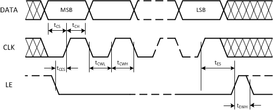
- The DATA is clocked into a shift register on each rising edge of the CLK signal. On the rising edge of the 24th CLK, the data is transferred from the data field to the selected register bank.
- The LE pin may be held high after programming, causing the LMX2571-EP to ignore clock pulses.
- When CLK or DATA lines are shared between devices, it is recommended to divide down the voltage to the CLK, DATA, and LE pins closer to the minimum voltage. This provides better noise immunity.
- If the CLK and DATA lines are toggled while the VCO is in lock, as is sometimes the case when these lines are shared with other parts, the phase noise may be degraded during the time of this programming.
 Figure 6-1 MICROWIRE Timing Diagram