JAJSM75G December   2015  – August 2022 LMX2592

PRODUCTION DATA  

  1. 特長
  2. アプリケーション
  3. 概要
  4. Revision History
  5. Pin Configuration and Functions
  6. Specifications
    1. 6.1 Absolute Maximum Ratings
    2. 6.2 ESD Ratings
    3. 6.3 Recommended Operating Conditions
    4. 6.4 Thermal Information
    5. 6.5 Electrical Characteristics
    6. 6.6 Timing Requirements
    7. 6.7 Typical Characteristics
  7. Detailed Description
    1. 7.1 Overview
    2. 7.2 Functional Block Diagram
    3. 7.3 Functional Description
      1. 7.3.1  Input Signal
      2. 7.3.2  Input Signal Path
      3. 7.3.3  PLL Phase Detector and Charge Pump
      4. 7.3.4  N Divider and Fractional Circuitry
      5. 7.3.5  Voltage Controlled Oscillator
      6. 7.3.6  VCO Calibration
      7. 7.3.7  VCO Doubler
      8. 7.3.8  Channel Divider
      9. 7.3.9  Output Distribution
      10. 7.3.10 Output Buffer
      11. 7.3.11 Phase Adjust
    4. 7.4 Device Functional Modes
      1. 7.4.1 Power Down
      2. 7.4.2 Lock Detect
      3. 7.4.3 Register Readback
    5. 7.5 Programming
      1. 7.5.1 Recommended Initial Power on Programming Sequence
      2. 7.5.2 Recommended Sequence for Changing Frequencies
    6. 7.6 Register Maps
      1. 7.6.1 LMX2592 Register Map – Default Values
        1. 7.6.1.1 Register Descriptions
  8. Application and Implementation
    1. 8.1 Application Information
      1. 8.1.1  Optimization of Spurs
        1. 8.1.1.1 Understanding Spurs by Offsets
        2. 8.1.1.2 Spur Mitigation Techniques
      2. 8.1.2  Configuring the Input Signal Path
        1. 8.1.2.1 Input Signal Noise Scaling
      3. 8.1.3  Input Pin Configuration
      4. 8.1.4  Using the OSCin Doubler
      5. 8.1.5  Using the Input Signal Path Components
        1. 8.1.5.1 Moving Phase Detector Frequency
        2. 8.1.5.2 Multiplying and Dividing by the Same Value
      6. 8.1.6  Designing for Output Power
      7. 8.1.7  Current Consumption Management
      8. 8.1.8  Decreasing Lock Time
      9. 8.1.9  Modeling and Understanding PLL FOM and Flicker Noise
      10. 8.1.10 External Loop Filter
    2. 8.2 Typical Application
      1. 8.2.1 Design for Low Jitter
        1. 8.2.1.1 Design Requirements
        2. 8.2.1.2 Detailed Design Procedure
        3. 8.2.1.3 Application Curve
    3. 8.3 Power Supply Recommendations
    4. 8.4 Layout
      1. 8.4.1 Layout Guidelines
      2. 8.4.2 Layout Example
  9. Device and Documentation Support
    1. 9.1 Device Support
      1. 9.1.1 Development Support
    2. 9.2 Documentation Support
      1. 9.2.1 Related Documentation
    3. 9.3 Receiving Notification of Documentation Updates
    4. 9.4 サポート・リソース
    5. 9.5 Trademarks
    6. 9.6 Electrostatic Discharge Caution
    7. 9.7 Glossary
  10. 10Mechanical, Packaging, and Orderable Information

パッケージ・オプション

デバイスごとのパッケージ図は、PDF版データシートをご参照ください。

メカニカル・データ(パッケージ|ピン)
  • RHA|40
サーマルパッド・メカニカル・データ
発注情報

External Loop Filter

The LMX2592 requires an external loop filter that is application-specific and can be configured by the PLLatinum™ simulation tool found here. For the LMX2592, it matters what impedance is seen from the Vtune pin looking outwards. This impedance is dominated by the component C3 for a third order filter or C1 for a second order filter. If there is at least 3.3 nF for the capacitance that is shunt with this pin, the VCO phase noise will be close to the best it can be. If there is less, the VCO phase noise in the 100-kHz to 1-MHz region will degrade. This capacitor should be placed close to the Vtune pin.
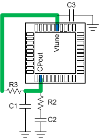
GUID-20210715-CA0I-GPKS-0HVC-GXTKGNFL61KS-low.gif Figure 8-10 External Loop Filter