JAJSM75G December 2015 – August 2022 LMX2592
PRODUCTION DATA
- 1 特長
- 2 アプリケーション
- 3 概要
- 4 Revision History
- 5 Pin Configuration and Functions
- 6 Specifications
- 7 Detailed Description
-
8 Application and Implementation
- 8.1
Application Information
- 8.1.1 Optimization of Spurs
- 8.1.2 Configuring the Input Signal Path
- 8.1.3 Input Pin Configuration
- 8.1.4 Using the OSCin Doubler
- 8.1.5 Using the Input Signal Path Components
- 8.1.6 Designing for Output Power
- 8.1.7 Current Consumption Management
- 8.1.8 Decreasing Lock Time
- 8.1.9 Modeling and Understanding PLL FOM and Flicker Noise
- 8.1.10 External Loop Filter
- 8.2 Typical Application
- 8.3 Power Supply Recommendations
- 8.4 Layout
- 8.1
Application Information
- 9 Device and Documentation Support
- 10Mechanical, Packaging, and Orderable Information
パッケージ・オプション
デバイスごとのパッケージ図は、PDF版データシートをご参照ください。
メカニカル・データ(パッケージ|ピン)
- RHA|40
サーマルパッド・メカニカル・データ
- RHA|40
発注情報
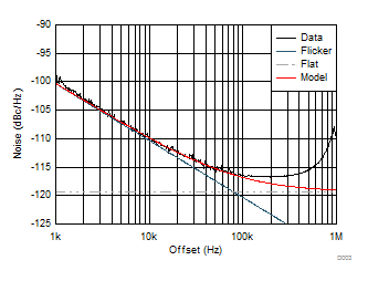
8.1.9 Modeling and Understanding PLL FOM and Flicker Noise
Follow these recommended settings to design for wide loop bandwidth and extract FOM and flicker noise. The flat model is the PLL noise floor modeled by: PLL_flat = PLL_FOM + 20 × log(Fvco/Fpd) + 10 × log(Fpd / 1 Hz). The flicker noise (also known as 1/f noise) which changes by –10dB / decade, is modeled by: PLL_flicker (offset) = PLL_flicker_Norm + 20 × log(Fvco / 1 GHz) – 10 × log(offset / 10k Hz). The cumulative model is the addition of both components: PLL_Noise = 10*log(10PLL_Flat / 10 + 10PLL_flicker / 10). This is adjusted to fit the measured data to extract the PLL_FOM and PLL_flicker_Norm spec numbers.
| PARAMETER | VALUE |
|---|---|
| PFD (MHz) | 200 |
| Charge pump (mA) | 12 |
| VCO frequency (MHz) | 5400 |
| Loop bandwidth (kHz) | 2000 |
| Phase margin (degrees) | 30 |
| Gamma | 1.4 |
| Loop filter (2nd order) | |
| C1 (nF) | 0.01 |
| C2 (nF) | 0.022 |
| R2 (kΩ) | 4.7 |
 Figure 8-9 FOM and Flicker Noise
Modeling