SNVS650H January 2010 – August 2015 LMZ12002
PRODUCTION DATA.
- 1 Features
- 2 Applications
- 3 Description
- 4 Revision History
- 5 Pin Configuration and Functions
- 6 Specifications
- 7 Detailed Description
- 8 Application and Implementation
- 9 Power Supply Recommendations
- 10Layout
- 11Device and Documentation Support
- 12Mechanical, Packaging, and Orderable Information
10 Layout
10.1 Layout Guidelines
PCB layout is an important part of DC-DC converter design. Poor board layout can disrupt the performance of a DC-DC converter and surrounding circuitry by contributing to EMI, ground bounce and resistive voltage drop in the traces. These can send erroneous signals to the DC-DC converter resulting in poor regulation or instability. Good layout can be implemented by following a few simple design rules.
- Minimize area of switched current loops.
- Have a single point ground.
- Minimize trace length to the FB pin.
- Make input and output bus connections as wide as possible.
- Provide adequate device heat-sinking.
From an EMI reduction standpoint, it is imperative to minimize the high di/dt current paths during PCB layout. The high current loops that do not overlap have high di/dt content that will cause observable high frequency noise on the output pin if the input capacitor CIN1 is placed a distance away for the LMZ12002. Therefore physically place CIN1 asa close as possible to the LMZ12002 VIN and GND exposed pad. This will minimize the high di/dt area and reduce radiated EMI. Additionally, grounding for both the input and output capacitor must consist of a localized top side plane that connects to the GND exposed pad (EP).
The ground connections for the feedback, soft-start, and enable components must be routed to the GND pin of the device. This prevents any switched or load currents from flowing in the analog ground traces. If not properly handled, poor grounding can result in degraded load regulation or erratic output voltage ripple behavior. Provide the single point ground connection from pin 4 to EP.
Both feedback resistors, RFBT and RFBB, and the feed forward capacitor CFF, must be located close to the FB pin. Since the FB node is high impedance, maintain the copper area as small as possible. The trace are from RFBT, RFBB, and CFF must be routed away from the body of the LMZ12002 to minimize noise.
This reduces any voltage drops on the input or output of the converter and maximizes efficiency. To optimize voltage accuracy at the load, ensure that a separate feedback voltage sense trace is made to the load. Doing so will correct for voltage drops and provide optimum output accuracy.
Use an array of heat-sinking vias to connect the exposed pad to the ground plane on the bottom PCB layer. If the PCB has a plurality of copper layers, these thermal vias can also be employed to make connection to inner layer heat-spreading ground planes. For best results use a 6 × 6 via array with a minimum via diameter of 8 mils thermal vias spaced 59 mils (1.5 mm). Ensure enough copper area is used for heat-sinking to keep the junction temperature below 125°C.
10.2 Layout Examples
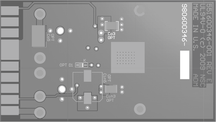
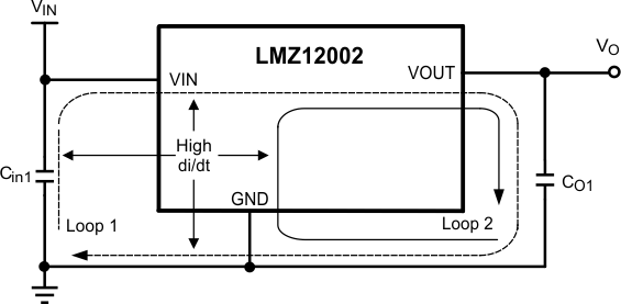 Figure 40. Critical Current Loops to Minimize
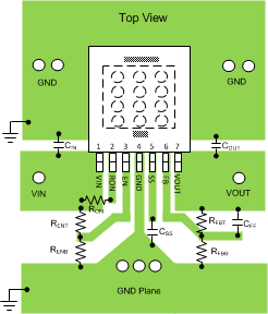 Figure 41. PCB Layout Guide
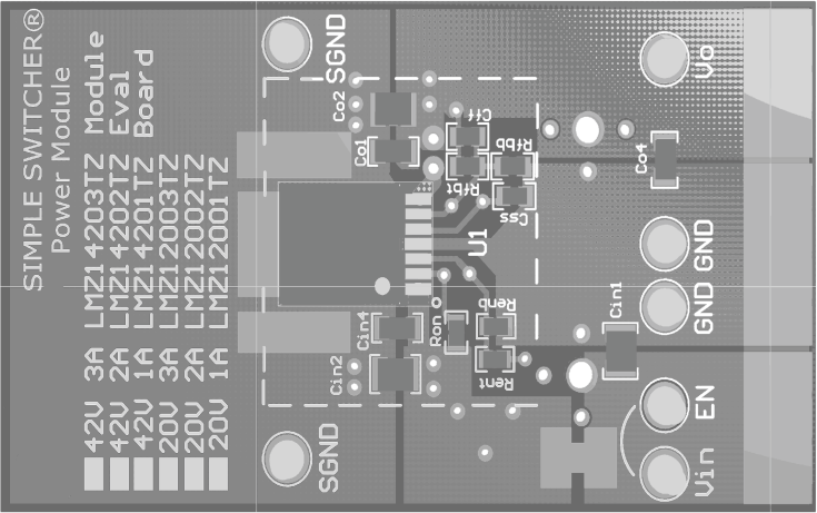 Figure 42. Top View of Evaluation PCB
10.3 Power Dissipation and Thermal Considerations
For the design case of VIN = 12 V, VO = 3.3 V, IO = 2 A, TAMB(MAX) = 85°C, and TJUNCTION = 125°C, the device must see a thermal resistance from case to ambient of:
Given the typical thermal resistance from junction to case to be 1.9°C/W. Use the 85°C power dissipation curves in the Typical Characteristics section to estimate the PIC-LOSS for the application being designed. In this application it is 1.2 W
To reach RθCA = 31.4, the PCB is required to dissipate heat effectively. With no airflow and no external heat, a good estimate of the required board area covered by 1-oz. copper on both the top and bottom metal layers is:
As a result, approximately 15.9 square cm of 1-oz. copper on top and bottom layers is required for the PCB design. The PCB copper heat sink must be connected to the exposed pad. Approximately thirty six, 8 mils thermal vias spaced 59 mils (1.5 mm) apart must connect the top copper to the bottom copper. For an example of a high thermal performance PCB layout, refer to the demo board application note AN-2024 (SNVA422).
10.4 Power Module SMT Guidelines
The recommendations below are for a standard module surface mount assembly
- Land Pattern — Follow the PCB land pattern with either soldermask defined or non-soldermask defined pads
- Stencil Aperture
- For the exposed die attach pad (DAP), adjust the stencil for approximately 80% coverage of the PCB land pattern
- For all other I/O pads use a 1:1 ratio between the aperture and the land pattern recommendation
- Solder Paste — Use a standard SAC Alloy such as SAC 305, type 3 or higher
- Stencil Thickness — 0.125 to 0.15 mm
- Reflow - Refer to solder paste supplier recommendation and optimized per board size and density
- Refer to Design Summary LMZ1xxx and LMZ2xxx Power Modules Family (SNAA214) for reflow information.
- Maximum number of reflows allowed is one
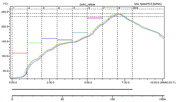 Figure 44. Sample Reflow Profile
Table 2. Sample Reflow Profile Table
| PROBE | MAX TEMP (°C) | REACHED MAX TEMP | TIME ABOVE 235°C | REACHED 235°C | TIME ABOVE 245°C | REACHED 245°C | TIME ABOVE 260°C | REACHED 260°C |
|---|---|---|---|---|---|---|---|---|
| 1 | 242.5 | 6.58 | 0.49 | 6.39 | 0.00 | – | 0.00 | – |
| 2 | 242.5 | 7.10 | 0.55 | 6.31 | 0.00 | 7.10 | 0.00 | – |
| 3 | 241.0 | 7.09 | 0.42 | 6.44 | 0.00 | – | 0.00 | – |
