JAJSF83E June 2013 – February 2020 LMZ31707
PRODUCTION DATA.
- 1 特長
- 2 アプリケーション
- 3 概要
- 4 改訂履歴
- 5 Specifications
- 6 Device Information
- 7 Typical Characteristics (PVIN = VIN = 12 V)
- 8 Typical Characteristics (PVIN = VIN = 5 V)
- 9 Typical Characteristics (PVIN = 3.3 V, VIN = 5 V)
-
10Application Information
- 10.1 Adjusting the Output Voltage
- 10.2 Capacitor Recommendations for the LMZ31707 Power Supply
- 10.3 Transient Response
- 10.4 Transient Waveforms
- 10.5 Application Schematics
- 10.6 Custom Design With WEBENCH® Tools
- 10.7 VIN and PVIN Input Voltage
- 10.8 3.3 V PVIN Operation
- 10.9 Power Good (PWRGD)
- 10.10 SYNC_OUT
- 10.11 Parallel Operation
- 10.12 Light Load Efficiency (LLE)
- 10.13 Power-Up Characteristics
- 10.14 Pre-Biased Start-up
- 10.15 Remote Sense
- 10.16 Thermal Shutdown
- 10.17 Output On/Off Inhibit (INH)
- 10.18 Slow Start (SS/TR)
- 10.19 Overcurrent Protection
- 10.20 Synchronization (CLK)
- 10.21 Sequencing (SS/TR)
- 10.22 Programmable Undervoltage Lockout (UVLO)
- 10.23 Layout Considerations
- 10.24 EMI
- 11デバイスおよびドキュメントのサポート
- 12メカニカル、パッケージ、および注文情報
10.17 Output On/Off Inhibit (INH)
The INH pin provides electrical on/off control of the device. Once the INH pin voltage exceeds the threshold voltage, the device starts operation. If the INH pin voltage is pulled below the threshold voltage, the regulator stops switching and enters low quiescent current state. The INH pin has an internal pullup current source, allowing the user to float the INH pin for enabling the device.
If an application requires controlling the INH pin, use an open drain/collector device, or a suitable logic gate to interface with the pin. Using a voltage superviser to control the INH pin allows control of the turnon and turnoff of the device as opposed to relying on the ramp up or down if the input voltage source.
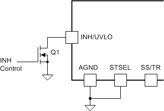
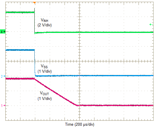
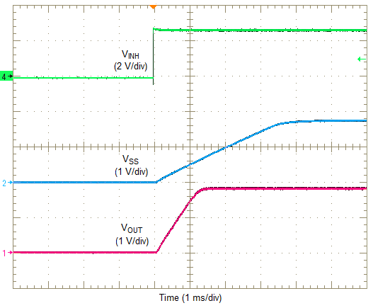
Figure 26 shows the typical application of the inhibit function. Turning Q1 on applies a low voltage to the inhibit control (INH) pin and disables the output of the supply, shown in Figure 27. If Q1 is turned off, the supply executes a soft-start power-up sequence, as shown in Figure 28. A regulated output voltage is produced within 2 ms. The waveforms were measured with a 5-A constant current load.
 Figure 26. Typical Inhibit Control
  Figure 27. Inhibit Turnoff
  Figure 28. Inhibit Turnon